Table of Contents
Advertisement
Quick Links
SERVICE MANUAL
Ver. 1.0 2008.12
System
Laser: Semiconductor laser
Signal format system: PAL/NTSC switchable
DVD/CD Player section
Signal-to-noise ratio: 120 dB
Frequency response: 10 – 20,000 Hz
Wow and flutter: Below measurable limit
Harmonic distortion: 0.01 %
Tuner section
FM
Tuning range:
AEP and UK models: 87.5 – 108.0 MHz
Russian model:
FM1/FM2: 87.5 – 108.0 MHz (at 50 kHz step)
FM3: 65 – 74 MHz (at 30 kHz step)
Asian model:
87.5 – 108.0 MHz (at 50 kHz step)
Latin American model:
87.5 – 107.9 MHz (at 200 kHz step)
Antenna (aerial) terminal:
External antenna (aerial) connector
Intermediate frequency: 10.7 MHz/450 kHz
Usable sensitivity: 9 dBf
Selectivity: 75 dB at 400 kHz
Signal-to-noise ratio: 67 dB (stereo), 69 dB (mono)
Harmonic distortion at 1 kHz: 0.5 % (stereo),
0.3 % (mono)
Separation: 35 dB at 1 kHz
Frequency response: 30 – 15,000 Hz
AM (E and Indian models)
Tuning range:
Asian model:
531 – 1,602 kHz (at 9 kHz step)
Latin American model:
530 – 1,710 kHz (at 10 kHz step)
Antenna (aerial) terminal:
External antenna (aerial) connector
Intermediate frequency: 10.7 MHz/450 kHz
Sensitivity: 30 μV
Sony Corporation
9-889-361-01
2008L05-1
Audio&Video Business Group
©
2008.12
Published by Sony Techno Create Corporation
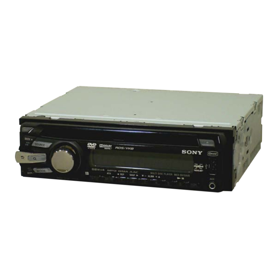
MEX-DV150UE/DV1500U/
Photo: MEX-DV150UE
SPECIFICATIONS
MW/LW (AEP, Russian and UK models)
Tuning range:
MW: 531 – 1,602 kHz
LW: 153 – 279 kHz
Antenna (aerial) terminal:
External antenna (aerial) connector
Intermediate frequency: 10.7 MHz/450 kHz
Sensitivity: MW: 30 μV, LW: 40 μV
USB Player section
Interface: USB (Full-speed)
Maximum current: 500mA
Power amplifier section
Outputs: Speaker outputs (sure seal connectors)
Speaker impedance: 4 – 8 ohms
Maximum power output: 52 W 4 (at 4 ohms)
General
Outputs:
Video output terminal
Rear audio output terminals
Power antenna (aerial) relay control terminal
Power amplifier control terminal
Inputs:
AUX audio input terminals
Antenna (aerial) input terminal
Parking break control terminal
AUX input jack (stereo mini jack)
USB signal input terminal
Tone controls:
Low: ±10 dB at 60 Hz
Mid: ±10 dB at 1 kHz
Hi: ±10 dB at 10 kHz
Russian Model
Model Name Using Similar Mechanism
Mechanism Type
Optical Pick-up Name
Power requirements: 12 V DC car battery
(negative ground (earth))
Dimensions: Approx. 178 50 179 mm
1
1
(7
/
2 7
8
Mounting dimensions: Approx. 182 53 163 mm
1
1
(7
/
2
/
4
8
Mass: Approx. 1.4 kg (3 lb 2 oz)
Supplied accessories:
Card remote commander: RM-X168
Parts for installation and connections (1 set)
Your dealer may not handle some of the above
listed accessories. Please ask the dealer for
detailed information.
US and foreign patents licensed from Dolby
Laboratories.
MPEG Layer-3 audio coding technology and
patents licensed from Fraunhofer IIS and
Thomson.
DivX, DivX Certified, and associated logos are
trademarks of DivX, Inc. and are used under
license.
This product is protected by certain intellectual
property rights of Microsoft Corporation. Use or
distribution of such technology outside of this
product is prohibited without a license from
Microsoft or an authorized Microsoft subsidiary.
Design and specifications are subject to change
without notice.
MULTI DISC PLAYER
DV1505U
AEP Model
UK Model
E Model
MEX-DV1500U
MEX-DV150UE
Indian Model
MEX-DV1505U
NEW
MG-612U-187
KHS-360A
/
in) (w/h/d)
8
1
6
/
in) (w/h/d)
2
Advertisement
Table of Contents

Related Manuals for Sony MEX-DV150UE


Summary of Contents for Sony MEX-DV150UE
- Page 1 530 – 1,710 kHz (at 10 kHz step) Antenna (aerial) terminal: MULTI DISC PLAYER External antenna (aerial) connector Intermediate frequency: 10.7 MHz/450 kHz Sensitivity: 30 μV Sony Corporation 9-889-361-01 2008L05-1 Audio&Video Business Group © 2008.12 Published by Sony Techno Create Corporation...
-
Page 2: Table Of Contents
COMPONENTS IDENTIFIED BY MARK 0 OR DOTTED LINE WITH MARK 0 ON THE SCHEMATIC DIAGRAMS AND IN THE PARTS LIST ARE CRITICAL TO SAFE OPERATION. REPLACE THESE COMPONENTS WITH SONY PARTS WHOSE PART NUMBERS APPEAR AS SHOWN IN THIS MANUAL OR IN SUPPLEMENTS PUBLISHED BY SONY. -
Page 3: Servicing Notes
MEX-DV150UE/DV1500U/DV1505U SECTION 1 SERVICING NOTES NOTE THE IC4 ON THE SERVO BOARD NOTES ON HANDLING THE OPTICAL PICK-UP REPLACING BLOCK OR BASE UNIT IC4 on the SERVO board cannot exchange with single. When this The laser diode in the optical pick-up block may suffer electrostat- part is damaged, exchange the entire mounted board. - Page 4 MEX-DV150UE/DV1500U/DV1505U EXTENSION CABLE AND SERVICE POSITION When repairing or servicing this set, connect the jig (extension cable) as shown below. • Connect the MAIN board (CN101) and the SERVO board (CN3) with the extension cable (Part No. J-2502-062-1). NOTE FOR FLEXIBLE BOARD OF THE OPTICAL...
- Page 5 MEX-DV150UE/DV1500U/DV1505U The following chart shows the supported compression formats, their file Playable discs and symbols used in this manual types, and the disc types on which those files can be stored. Available functions differ depending on the format, regardless of disc This unit can play various video/audio discs.
-
Page 6: General
MEX-DV150UE/DV1500U/DV1505U SECTION 2 This section is extracted GENERAL from instruction manual. (DV1500U: E model/DV1505U) Location and function of controls Main unit MODE button To select the radio band (FM/AM); select an auxiliary device connected to the AUX input jack (front) or AUX IN jack (rear). - Page 7 MEX-DV150UE/DV1500U/DV1505U (DV150UE/DV1500U: AEP and UK models) Location and function of controls Main unit MODE button To select the radio band (FM/MW/LW); select an auxiliary device connected to the AUX input jack (front) or AUX IN jack (rear). Receptor for the card remote commander...
- Page 8 MEX-DV150UE/DV1500U/DV1505U (DV1500U: E model/DV1505U) Cautions • This unit is designed for negative ground (earth) 12 V DC operation only. • Do not get the leads under a screw, or caught in moving parts (e.g. seat railing). FRONT • Before making connections, turn the car ignition off to AUDIO OUT avoid short circuits.
- Page 9 The mounting position El gancho debe encontrarse of the parking brake switch cord depends on your car. en la parte interior. Consult your car dealer or your nearest Sony dealer for further details. ...
- Page 10 MEX-DV150UE/DV1500U/DV1505U (DV150UE/DV1500U: AEP and UK models) VIDEO OUT FRONT Monitor* AUDIO OUT Monitor* Moniteur* Monitor* Monitor* Monitor* Monitor* Moniteur* Monitor* Monitor* REAR / SUB AUDIO OUT * not supplied nicht mitgeliefert non fourni non in dotazione niet bijgeleverd * not supplied...
- Page 11 Power connection diagram brake switch cord. The mounting position of the parking brake switch cord depends on your car. Consult your car dealer or your nearest Sony dealer for further details. Auxiliary power connector may vary depending on the car. Check your...
-
Page 12: Disassembly
MEX-DV150UE/DV1500U/DV1505U SECTION 3 DISASSEMBLY • This set can be disassembled in the order shown below. 3-1. DISASSEMBLY FLOW FRONT PANEL SECTION Note: Illustration of disassembly is omitted. 3-2. SUB PANEL COMPLETE ASSY (Page 12) 3-3. DVD MECHANISM DECK BLOCK (Page 13) 3-4. -
Page 13: Dvd Mechanism Deck Block
MEX-DV150UE/DV1500U/DV1505U 3-3. DVD MECHANISM DECK BLOCK dust protection sheet bracket (CD) DVD mechanism deck block connector (CN3) screw (PTT2.6 × 6) laser caution label two screws (PTT2.6 × 5) connector (CN702) shield (612Z) two screws (P1.7 × 2.2) screw (PTT2.6 × 6) Lift up the DVD mechanism deck (MG-612U-187). -
Page 14: Chassis (T612Z) Sub Assy, Sensor Board
MEX-DV150UE/DV1500U/DV1505U 3-5. CHASSIS (T612Z) SUB ASSY, SENSOR BOARD claw two screws two screws (P1.7 × 2.2) (P1.7 × 2.2) chassis (T612Z) sub assy Remove the three solders. SENSOR borad claw 3-6. CHASSIS (OP, ZA) COMPLETE ASSY chassis (OP, ZA) complete assy... -
Page 15: Servo Board
MEX-DV150UE/DV1500U/DV1505U 3-7. SERVO BOARD OP flexible board (CN2) Note: When disconnecting the OP flexible board from of the connector. Be sure to refer to “NOTE FOR FLEXIBLE BOARD OF THE OPTICAL PICK-UP” of the servicing notes (See page 4). four screws (M1.7 ×... -
Page 16: Electrical Check
MEX-DV150UE/DV1500U/DV1505U SECTION 4 ELECTRICAL CHECK Check Location: SERVO SECTION – SERVO Board (Conductor Side) – If any of the following parts was replaced, perform the “IOP Check” as mentioned below. • Optical pick-up block (chassis (OP, ZA) complete assy TP47 •... -
Page 17: Diagrams
MEX-DV150UE/DV1500U/DV1505U SECTION 5 DIAGRAMS 5-1. BLOCK DIAGRAM - SERVO/VIDEO/USB Section - OPTICAL PICK-UP BLOCK DVD PROCESSOR D/A CONVERTER KHS-360A (Page 18) 193 RFP AOUT0 6 DATA RF– R-CH R-ch is omitted due to same as L-ch. AMCLK 5 SCK 196 A... -
Page 18: Block Diagram - Tuner/Audio Section
MEX-DV150UE/DV1500U/DV1505U 5-2. BLOCK DIAGRAM - TUNER/AUDIO Section - CN652 (FRONT AUDIO OUT) R-CH REAR/SUB AUDIO OUT R-CH INPUT SELECTOR, POWER AMP AUDIO PROCESSOR IC802 (1/2) CN801 (1/2) IC302 LINE AMP FL RR+ 5 (Page 17) 2 DVD-L FL 34 12 FL IN_RR IC301 FL RR–... -
Page 19: Block Diagram - Panel/Power Supply Section
MEX-DV150UE/DV1500U/DV1505U 5-3. BLOCK DIAGRAM - PANEL/POWER SUPPLY Section - M850 (FAN) +1.8V D+1.8V REGULATOR IC101 +3.3V REGULATOR VIDEO +3.3V REGULATOR IC802 (2/2) LCD DRIVER SYSTEM CONTROLLER IC17 IC901 IC503 (3/3) DR+5V 33 REG4 LCD_SO LCD_CKO S1 – S48 TU +5V... - Page 20 MEX-DV150UE/DV1500U/DV1505U THIS NOTE IS COMMON FOR PRINTED WIRING BOARDS AND SCHEMATIC DIAGRAMS. • Circuit Boards Location (In addition to this, the necessary note is printed in each block.) For Printed Wiring Boards. For Schematic Diagrams. Note: Note: • X : Parts extracted from the component side.
-
Page 21: Schematic Diagram - Servo Section (1/3)
MEX-DV150UE/DV1500U/DV1505U 5-4. SCHEMATIC DIAGRAM - SERVO Section (1/3) - • See page 32 for IC Block Diagrams. (1/3) FCS+ TRK+ TRK- FCS- C160 0.0047 VR(DVD) C162 0.001 VR(CD) 2SK3018-T106 LD(DVD) CD ON SWITCH LD(DVD) GND(LD COM) DTC114EE-TL GND(LD COM) 2SK3018-T106... -
Page 22: Schematic Diagram - Servo Section (2/3)
MEX-DV150UE/DV1500U/DV1505U 5-5. SCHEMATIC DIAGRAM - SERVO Section (2/3) - • See page 32 for Waveforms. • See page 39 for IC Pin Function Description. (2/3) IC17 S-1206B33-U3T1G R121 +3.3V REGULATOR VGND A+5V D+1.8V (Page 23) D+3.3V 27MHz 1.2k 4.7k FB31 FB23 0.01... -
Page 23: Schematic Diagram - Servo Section (3/3)
MEX-DV150UE/DV1500U/DV1505U 5-6. SCHEMATIC DIAGRAM - SERVO Section (3/3) - • See page 32 for IC Block Diagrams. (3/3) SDRAM_DAT(15:0) SDRAM_CNT SDRAM_ADD MEMRD SD-RAM C135 MEMDAT(15:0) IC10 C134 0.01 EM638165TS-6G MEMADD(20:0) C133 MEMADD16 MEMWR RB119 RB122 (Page 22) SDRAMGND DQ15 FLASH MEMORY... -
Page 24: Printed Wiring Boards - Servo Section
MEX-DV150UE/DV1500U/DV1505U 5-7. PRINTED WIRING BOARDS - SERVO Section - • See page 20 for Circuit Boards Location. • : Uses unleaded solder. • Semiconductor SERVO BOARD SERVO BOARD (COMPONENT SIDE) (CONDUCTOR SIDE) Location Ref. No. Location R136 R134 R135 TP31... -
Page 25: Schematic Diagram - Main Board (1/3)
MEX-DV150UE/DV1500U/DV1505U 5-8. SCHEMATIC DIAGRAM - MAIN Board (1/3) - • See page 32 for IC Block Diagrams. PJ651 PJ601 AUX IN VIDEO OUT (1/3) (CHASSIS) TP202 D601 MAZ8068GML J201 (ANTENNA IN) C601 TUX-201 0.001 R653 TUX-032//Q3 C602 VD601 DV150UE/ 0.0047... -
Page 26: Schematic Diagram - Main Board (2/3)
MEX-DV150UE/DV1500U/DV1505U 5-9. SCHEMATIC DIAGRAM - MAIN Board (2/3) - • See page 32 for Waveforms. • See page 32 for IC Block Diagrams. • See page 39 for IC Pin Function Description. (Page 25) (2/3) IC151 NJM2561F1 VIDEO AMP C157... -
Page 27: Schematic Diagram - Main Board (3/3)
MEX-DV150UE/DV1500U/DV1505U 5-10. SCHEMATIC DIAGRAM - MAIN Board (3/3) - • See page 32 for Waveforms. • See page 32 for IC Block Diagrams. (DV1500U: E/DV1505U) TP801 CN801 (3/3) DV1500U: E/ FRONT LCH (-) TP809 DV1505U FRONT LCH (+) TP802 REAR LCH (-) -
Page 28: Printed Wiring Board - Main Board (Component Side)
MEX-DV150UE/DV1500U/DV1505U • See page 20 for Circuit Boards Location. 5-11. PRINTED WIRING BOARD - MAIN Board (Component Side) - • : Uses unleaded solder. • Semiconductor Location Ref. No. Location D501 D502 D503 D504 MAIN BOARD (COMPONENT SIDE) D801 D802... -
Page 29: Printed Wiring Board - Main Board (Conductor Side)
MEX-DV150UE/DV1500U/DV1505U • See page 20 for Circuit Boards Location. 5-12. PRINTED WIRING BOARD - MAIN Board (Conductor Side) - • : Uses unleaded solder. • Semiconductor Location Ref. No. Location D103 D201 REAR/SUB FRONT AUDIO OUT AUDIO OUT D361 MAIN BOARD... -
Page 30: 5-13. Printed Wiring Boards - Key Section
MEX-DV150UE/DV1500U/DV1505U 5-13. PRINTED WIRING BOARDS - KEY Section - • See page 20 for Circuit Boards Location. • : Uses unleaded solder. • Semiconductor Location Ref. No. Location D901 LSW901, 905 – 913 KEY BOARD (COMPONENT SIDE) S902 – 908 D902 LED907, 911, 913 –... -
Page 31: 5-14. Schematic Diagram - Key Section
MEX-DV150UE/DV1500U/DV1505U 5-14. SCHEMATIC DIAGRAM - KEY Section - • See page 32 for IC Block Diagrams. JACK BOARD KEY BOARD FB901 R905 R907 W001 W004 W003 W005 FB902 LED901 W002 W006 J901 NESW505CT-AST R906 FB903 BACK LIGHT LSW905 DSPL R935... - Page 32 MEX-DV150UE/DV1500U/DV1505U • Waveforms • IC Block Diagrams – SERVO Board – – MAIN Board – – SERVO Board – IC1 BH6599KV-E2 (ALRCLK) IC503 (XCOUT) 32 31 29 28 26 25 STBY STANDBY 3.9 Vp-p SHORT 2.9 Vp-p DRIVER DRIVER DRIVER...
- Page 33 MEX-DV150UE/DV1500U/DV1505U IC10 EM638165TS-6G VDD 1 DQ0 2 DQ15 VDDQ 3 VSSQ DQ1 4 DQ14 DQ2 5 DQ13 1M × 16 VSSQ 6 CELL ARRAY VDDQ (BANK #A) DQ3 7 DQ12 DQ4 8 COLUMN DECODER DQ11 VDDQ 9 VSSQ DQ5 10...
- Page 34 MEX-DV150UE/DV1500U/DV1505U – MAIN Board – IC103 NJM2387ADL3 (TE2) IC102 BD7931F REGULATOR OVER VOLTAGE OVER CURRENT CONTROL PROTECTION PROTECTION LOGIC BANDGAP REFERENCE POWER CMOS THERMAL THERMAL H-BRIDGE SHUT-DOWN ON/OFF PROTECTION CONTROL IC151 NJM2561F1-TE2 POWER SAVE LOW-PASS 75 OHM VOUT FILTER DRIVER...
- Page 35 MEX-DV150UE/DV1500U/DV1505U IC302 BD3447AFV-E2 I2C BUS LOGIC, FADER FADER FADER FADER FADER EFFECT 180°/0° 7 BAND 3 BAND P-EQ (TONE CONTROL) SPECTRUM ANALYZER /LEVEL METER VOLUME/MUTE SPEANA LVL METER LVL METER SPEANA INPUT GAIN INPUT SELECTOR (3 SIGLE-END AND 3 STEREO IS O)
- Page 36 MEX-DV150UE/DV1500U/DV1505U IC401 BD9778HFP SOFT VREF START ERROR LATCH COMPARATOR CURRENT LIMIT DRIVER THERMAL SHUT DOWN IC402 TPS2051BDRG4 CHARGE PUMP CURRENT DRIVER LIMIT UVLO THERMAL SENCE IC431 S-1170B33UC-OTSTFG VOUT OVERCURRENT PROTECTION THERMAL SHUTDOWN ON/OFF ON/OFF CONTROL – REFERENCE VOLTAGE...
- Page 37 MEX-DV150UE/DV1500U/DV1505U IC802 TDA8588J/N2/R1 PGND2/TAB 1 OUT3– 3 MUTING OUT3+ 5 OUT1– 7 PGND1 MUTING OUT1+ 9 SGND 13 IN2 15 ACGND OUT2+ 17 MUTING PGND3 OUT2– 19 OUT4+ 21 MUTING OUT4– 23 STANDBY/ PGND4 MUTING DIAG 25 PROTECTION/ DIAGNOSTIC IIC-BUS INTERFACE TEMPERATURE &...
- Page 38 MEX-DV150UE/DV1500U/DV1505U – KEY Board – IC901 LC75826WH-US-E 59 58 57 56 54 53 52 51 50 49 COMMON DRIVER CCB INTERFACE CLOCK GENERATOR SHIFT REGISTER P1/S1 48 S48 47 S47 P2/S2 46 S46 P3/S3 CONTROL REGISTER P4/S4 45 S45 P5/S5...
- Page 39 MEX-DV150UE/DV1500U/DV1505U • IC Pin Function Description SERVO BOARD IC4 ZR36886HLCG-A (DVD PROCESSOR) Pin No. Pin Name Description 1 to 7 NOT USED Not used SSCCLK Serial data transfer clock signal input terminal Not used SSCTXD Serial data output terminal Not used...
- Page 40 MEX-DV150UE/DV1500U/DV1505U Pin No. Pin Name Description VDDUSB Power supply terminal (+3.3V) USBDP USB data (positive) input from the USB connector USBDN USB data (negative) input from the USB connector GNDUSB Ground terminal RAMADD4, RAMADD3, 69 to 73 RAMADD5, Address signal output to the SD-RAM...
- Page 41 MEX-DV150UE/DV1500U/DV1505U Pin No. Pin Name Description IDGPCIO0 Serial data output to the D/A converter NOT USED Not used 127, 128 AOUT2, AOUT1 Audio data output terminal Not used AOUT0 Audio data output to the D/A converter AIN2 Chip select signal output to the D/A converter...
- Page 42 MEX-DV150UE/DV1500U/DV1505U Pin No. Pin Name Description K signal input terminal Not used F signal input from the optical pick-up block Reference voltage (+1.65V) output to the optical pick-up block VBGAP Bandgap reference input terminal RESOUT Internal reference output terminal CD_MD...
- Page 43 MEX-DV150UE/DV1500U/DV1505U MAIN BOARD IC503 R5F3640DDZ98FB (SYSTEM CONTROLLER) Pin No. Pin Name Description FSW_IN Oscillation frequency count signal input from the DC/DC converter SIRCS_IN SIRCS signal input from the remote control receiver LCD_SO Data output to the liquid crystal display driver...
- Page 44 MEX-DV150UE/DV1500U/DV1505U Pin No. Pin Name Description Chucking end detection switch input terminal M_RESET Reset signal output to the DVD processor and fl ash memory "L": reset M_CTS Data communication request signal output to the DVD processor 58, 59 Not used Power supply terminal (+3.3V)
-
Page 45: Exploded Views
MEX-DV150UE/DV1500U/DV1505U SECTION 6 EXPLODED VIEWS Note: • -XX and -X mean standardized parts, so • The mechanical parts with no reference The components identifi ed by mark 0 they may have some difference from the number in the exploded views are not sup- or dotted line with mark 0 are critical for original one. -
Page 46: Front Panel Section
MEX-DV150UE/DV1500U/DV1505U 6-2. FRONT PANEL SECTION not supplied (KEY board) RE901 CN901 not supplied not supplied not supplied (JACK board) J901 not supplied LCD901 CN902 not supplied not supplied not supplied not supplied not supplied not supplied Note: Refer to the servicing notes “NOTE FOR REPLACEMENT OF THE USB CONNECTOR (CN902)”... -
Page 47: Dvd Mechanism Deck Section (Mg-612U-187)
MEX-DV150UE/DV1500U/DV1505U 6-3. DVD MECHANISM DECK SECTION (MG-612U-187) not supplied not supplied not supplied (SENSOR board) not supplied not supplied Ref. No. Part No. Description Remark Ref. No. Part No. Description Remark A-1211-766-B CHASSIS (T612Z) SUB ASSY 3-259-033-01 DAMPER (S) 4-108-794-01... -
Page 48: Electrical Parts List
MEX-DV150UE/DV1500U/DV1505U SECTION 7 JACK ELECTRICAL PARTS LIST Note: • Due to standardization, replacements in • COILS When indicating parts by reference num- the parts list may be different from the uH: μH ber, please include the board name. parts specifi ed in the diagrams or the com- •... - Page 49 MEX-DV150UE/DV1500U/DV1505U MAIN Ref. No. Part No. Description Remark Ref. No. Part No. Description Remark R914 1-216-864-11 SHORT CHIP < VARISTOR > R920 1-216-820-11 METAL CHIP 1/10W R921 1-216-821-11 METAL CHIP 1/10W VDR900 1-804-988-21 VARISTOR, CHIP (1608) R922 1-216-821-11 METAL CHIP...
- Page 50 MEX-DV150UE/DV1500U/DV1505U MAIN Ref. No. Part No. Description Remark Ref. No. Part No. Description Remark C221 1-107-826-11 CERAMIC CHIP 0.1uF C532 1-125-972-61 ELECT 100uF C581 1-107-826-11 CERAMIC CHIP 0.1uF C225 1-107-826-11 CERAMIC CHIP 0.1uF C582 1-107-826-11 CERAMIC CHIP 0.1uF (DV150UE/DV1500U: AEP, UK)
- Page 51 MEX-DV150UE/DV1500U/DV1505U MAIN Ref. No. Part No. Description Remark Ref. No. Part No. Description Remark < CONNECTOR > FB103 1-500-283-11 INDUCTOR, FERRITE BEAD FB105 1-469-179-21 INDUCTOR, FERRITE BEAD CN101 1-821-736-11 CONNECTOR, BOARD TO BOARD 30P FB106 1-469-179-21 INDUCTOR, FERRITE BEAD CN501...
- Page 52 MEX-DV150UE/DV1500U/DV1505U MAIN Ref. No. Part No. Description Remark Ref. No. Part No. Description Remark Q203 6-551-696-01 TRANSISTOR ISA1235AC1TP-1EF R319 1-216-809-11 METAL CHIP 1/10W (DV150UE/DV1500U: AEP, UK) R320 1-216-809-11 METAL CHIP 1/10W Q204 8-729-038-28 TRANSISTOR RT1N441C-TP-1 R321 1-216-809-11 METAL CHIP 1/10W...
- Page 53 MEX-DV150UE/DV1500U/DV1505U MAIN SENSOR SERVO Ref. No. Part No. Description Remark Ref. No. Part No. Description Remark R524 1-216-845-11 METAL CHIP 100K 1/10W R803 1-216-073-91 METAL CHIP 1/10W R525 1-216-845-11 METAL CHIP 100K 1/10W R811 1-216-841-11 METAL CHIP 1/10W R526 1-216-809-11...
- Page 54 MEX-DV150UE/DV1500U/DV1505U SERVO Ref. No. Part No. Description Remark Ref. No. Part No. Description Remark 1-135-856-91 TANTALUM CHIP 100uF 1-100-567-81 CERAMIC CHIP 0.01uF 1-164-937-11 CERAMIC CHIP 0.001uF 1-125-777-11 CERAMIC CHIP 0.1uF 1-125-777-11 CERAMIC CHIP 0.1uF 1-100-567-81 CERAMIC CHIP 0.01uF 1-112-672-81 CERAMIC CHIP 330PF 1-125-777-11 CERAMIC CHIP 0.1uF...
- Page 55 MEX-DV150UE/DV1500U/DV1505U SERVO Ref. No. Part No. Description Remark Ref. No. Part No. Description Remark 1-691-394-61 CONNECTOR, FFC/FPC (ZIF) 30P 1-218-937-11 METAL CHIP 1/16W 1-815-352-11 CONNECTOR, BOARD TO BOARD 30P 1-218-973-11 METAL CHIP 1/16W 1-580-056-21 PIN, CONNECTOR (SMD) 3P 1-218-941-81 METAL CHIP...
- Page 56 MEX-DV150UE/DV1500U/DV1505U SERVO Ref. No. Part No. Description Remark Ref. No. Part No. Description Remark R134 1-216-864-11 SHORT CHIP MISCELLANEOUS R135 1-216-864-11 SHORT CHIP ************** R136 1-216-864-11 SHORT CHIP R159 1-218-941-81 METAL CHIP 1/16W 1-828-543-21 CORD (WITH CONNECTOR) (POWER) (DV1500U: AEP, UK/DV150UE)
- Page 57 MEX-DV150UE/DV1500U/DV1505U Ref. No. Part No. Description Remark PARTS FOR INSTALLATION AND CONNECTIONS ************************************** X-2179-431-2 FRAME ASSY, FITTING 3-876-675-01 KEY (FRAME) 3-873-543-02 COLLAR 1-828-543-21 CORD (WITH CONNECTOR) (POWER) (DV1500U: AEP, UK/DV150UE) KEY (FRAME) COLLAR 1-833-970-21 CONNECTION CODE FOR AUTOMOBILE × 2 ×...
- Page 58 MEX-DV150UE/DV1500U/DV1505U REVISION HISTORY Checking the version allows you to jump to the revised page. Also, clicking the version at the top of the revised page allows you to jump to the next revised page. Ver. Date Description of Revision 2008.12...