Sony BC-1WD Service Manual
Hide thumbs
Also See for BC-1WD:
- Operating instructions manual (37 pages) ,
- Operation and maintenance manual (58 pages)
Table of Contents
Advertisement
Advertisement
Table of Contents

Related Manuals for Sony BC-1WD


Summary of Contents for Sony BC-1WD
- Page 1 BATTERY CHARGER BC-1WD BC-1WDCE SERVICE MANUAL 1st Edition...
- Page 2 Ce manual est destiné uniquement aux personnes compétentes en charge de l’entretien. Afin de réduire les risques de décharge électrique, d’incendie ou de blessure n’effectuer que les réparations indiquées dans le mode d’emploi à moins d’être qualifié pour en effectuer d’autres. Pour toute réparation faire appel à une personne compétente uniquement. BC-1WD...
-
Page 3: Table Of Contents
Schematic Diagram ..................6-2 7. Board Layouts A board (CK-2847) ..................7-1 B board (CK-2848) ..................7-1 C board (CK-2849) ..................7-2 C board (CK-4406) ..................7-2 D board (CK-2853) ..................7-2 E board (CK-2884) ..................7-2 1 (E) BC-1WD... - Page 5 This symbol is intended to alert the user to the presence of important operating and maintenance (servicing) instructions in the literature accompanying the appliance. BC-1WD BC-1WDCE © 1993 Sony Corporation...
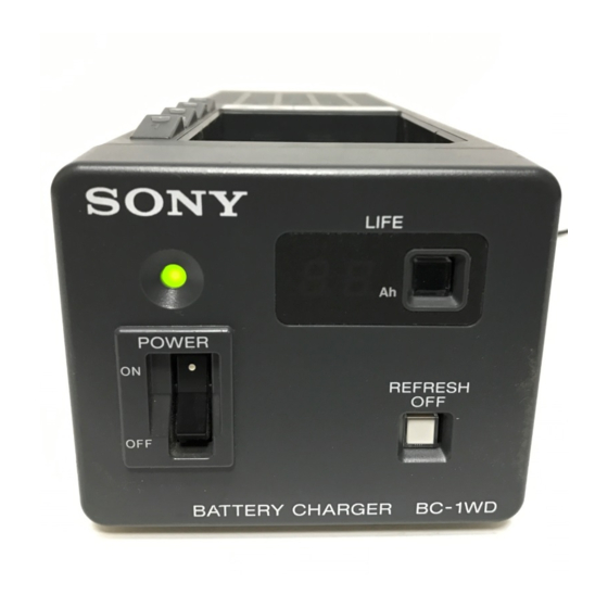
- Page 6 Table of Contents Overview The BC-1WD/1WDCE is a battery charger capable of Overview ............14 Charging System continuous charging, into which any four NP-1/1A/1B Locations and Functions of Parts ....16 battery packs can be inserted simultaneously. The BC-1WD/1WDCE begins discharging once the Charging ............
- Page 7 Lamp Status Meaning Slowly flashing in Auto refresh in progress (fully discharging the battery) Lit in red End of auto refresh Booster charge in progress Slowly flashing in green Near end of booster charge Rapidly flashing in green Lit in green End of booster charge or trickle charge in progress Lit alternately in...
- Page 8 Applicable battery packs and charging time Battery pack life judgement Power requirement BC-1WD: 120 V AC, 60 Hz The capacity of the battery pack in section 4 is The time needed to charge one fully discharged battery BC-1WDCE: 220 to 240 V pack is as follows.
-
Page 9: Service Overview
(2) Disconnect the connector CN3 from the A board. (3) Disconnect the connector CN5 from the C board. 3. Removal of the front cover (1) Remove the five screws 4 and two screws 5. (2) Disconnect the connector CN1 from the A board. 2-1 (E) BC-1WD... -
Page 10: Location Of Printed Circuit Boards
2-2. Location of Printed Circuit Boards 2-2. Location of Printed Circuit Boards 2-2 (E) BC-1WD... -
Page 11: Alignment
3. Adjust the 1VR103 so that the DC current between terminals is 2.0 ± 0.05 A. If it is hard to get the following parts, constitute an equiva- lent circuit. VR103 VR101 VR102 A board (A side) 3-1 (E) BC-1WD... -
Page 13: Spare Parts
Therefore, specified parts should be used in the case of replacement. 2. Standardization of Parts Some repair parts supplied by Sony differ from those used for the unit. These are because of parts common- ality and improvement. Parts list has the present standardized repair parts. - Page 15 Part No. SP Description Part No. SP Description 2-990-241-02 o HOLDER(A),PLUG 7-623-423-07 s WASHER LW4(TYPE B) 9-905-407-02 o MOUNTED CIRCUIT BOARD,A (FOR J) 7-682-548-04 s SCREW +B 3X8 9-905-408-02 o MOUNTED CIRCUIT BOARD,A (FOR UC) 7-682-548-09 s SCREW +B 3X8 9-905-409-02 o MOUNTED CIRCUIT BOARD,A (FOR EK) 7-682-553-04 s SCREW +B 3X20 9-905-410-01 o MOUNTED CIRCUIT BOARD,B...
-
Page 16: Electrical Parts List
RY106 9-905-452-01 s 12V,APA3311 RY107 9-905-452-01 s 12V,APA3311 9-905-626-01 o HOLDER,FUSE RY108 9-905-452-01 s 12V,APA3311 IC101 9-905-442-01 s FA5311P T101 9-905-453-01 s ETS33AC1H6AC IC102 8-759-159-01 s UPC24M10HF IC103 9-905-443-01 s L78MG TH101 9-905-454-01 s 5D-11 IC107 8-759-708-05 s NJM78L05A BC-1WD... -
Page 17: B Board(Ck-2848)
1-249-409-11 s CARBON 220 1/4W R219 1-247-855-11 s CARBON 10K 1/4W S201 9-905-638-01 s SWITCH S202 9-905-639-01 s SWITCH 9-905-640-01 s KEY TOP(WHITE) 9-905-641-01 s KEY TOP(BLACK) 2pcs 9-905-642-01 s CAP 9-905-643-01 s COLLAR CHIP(WHITE) 9-905-644-01 s COLLAR CHIP(BLACK) BC-1WD... -
Page 18: C Board (Ck-2849)
1-216-045-00 s CHIP 680 1/10W 8-759-510-71 s BA10358F-E2 1-216-045-00 s CHIP 680 1/10W 8-759-100-93 s UPC393G2 IC10 8-759-501-10 s SN74LS540NS 1-216-045-00 s CHIP 680 1/10W IC11 9-905-467-01 s TD62084F 1-216-045-00 s CHIP 680 1/10W IC12 9-905-468-01 s S-8054ALR-LN-X 1-216-073-00 s CHIP 10K 1/10W BC-1WD... -
Page 19: D Board (Ck-2853)
8-719-420-90 s MA8051-M 8-719-420-90 s MA8051-M 8-719-420-90 s MA8051-M 8-719-420-90 s MA8051-M 8-719-420-90 s MA8051-M 8-719-420-90 s MA8051-M 8-719-420-90 s MA8051-M 8-719-018-03 s MA8240 ZD10 8-719-018-03 s MA8240 ZD11 8-719-018-03 s MA8240 ZD12 8-719-018-03 s MA8240 ZD13 8-719-422-70 s MA8075 BC-1WD... -
Page 20: E Board(Ck-2884)
Ref. No. 9-905-475-01 o LED HOLDER or Q’ty Part No. SP Description 9-905-658-01 o LED CABLE ASSY 1-782-059-11 s CORD,POWER(FOR J) 1-551-812-11 s CORD,POWER(FOR UC) 1-782-929-11 s CORD,POWER(BS 3P) (FOR EK) 2-990-242-01 o HOLDER(B),PLUG(FOR J,UC) 3-613-640-01 o HOLDER(C),PLUG(FOR EK) BC-1WD... - Page 21 PC111 ......5-3 RD-20FB ......5-2 UPC324G2 ....... 5-6 RD-30EB ......5-2 PC111YS ......5-3 UPC339G2 ....... 5-4 RD-30FB ......5-2 UPC358G2 ....... 5-3 RD-4.3ES ......5-2 UPC393G2 ....... 5-6 UPC78L05J ...... 5-4 S3WB60 ......5-2 UPC78L10T ..... 5-6 BC-1WD...
- Page 22 —BOTTOM VIEW— S3WB60 ERA91-02 2SK960 ESAB82M-004 —TOP VIEW— ESAC92M-02 18 17 16 15 14 13 12 11 10 LN5230KMOS 2 3 4 5 6 7 8 9 2SK982 —TOP VIEW— MA113-(TX) MA729 TYPE NO. MA175WK PRINTED DTC114ES (R1=10k,R2=10k) UN4211 BC-1WD...
- Page 23 : GENERATOR TIMING RESISTOR OUTPUTS : FEEDBACK : DRIVE UNDER VOLTAGE LOCKOUT BIAS 7.0 V 3.6 V 2.8 V Dmax (46%, 70%) COMPARATOR IS (+) 0.24 V OVER-CURRENT NOTE PROTECTION FA5310 : Dmax = 46% FA5311 : Dmax = 70% BC-1WD...
- Page 24 MOD0 - MOD1 P32/SI INTERFACE EXTERNAL 14,15 P35/INT1 PORT2 P22,P23 INTERRUPTION C-MOS P36/INT2 10-13,16,17 OUTPUT P37/BZ/RCO PORT P27 - 24, P21, P20 N CH OPEN 45-48 DRAIN (128 x 8-BIT) P43/AN3 - P40/AN0 OUTPUT PORT MC-8L 8-BIT (4K x 8-BIT) CONVERTER BC-1WD...
- Page 25 A B C D TEST LATCH LATCH LATCH LATCH Y = A • B = A + B CARRY A1 B1 C1 D1 UP/DOWN UP/DOWN UP/DOWN DECADE DECADE DECADE : LOW LEVEL COUNTER COUNTER COUNTER DOWN : HIGH LEVEL BORROW BC-1WD...
- Page 26 UPC78L10T (NEC)+10V POSITIVE VOLTAGE REGULATOR —TOP VIEW— COMMON OUTPUT 10.5 k INPUT 7.2 k UPC24M10HF (NEC)+10V(0.5A) POSITIVE VOLTAGE REGULATOR —FRONT VIEW— INPUT OUTPUT INPUT OUTPUT UPC324G2 (NEC) QUAD OPERATIONAL AMPLIFIERS —TOP VIEW— OUT IN_ IN_ OUT OUT IN_ IN_ OUT BC-1WD...
- Page 27 Overall Overall Section 6 Diagrams 6-1. Block Diagram BC-1WD (UC) : S/N 20001 and Higher BC-1WD (J) : S/N 10001 and Higher BC-1WD (EK) : S/N 30001 and Higher Overall BC-1WD...
- Page 28 Frame Wiring Frame Wiring 6-2. Schematic Diagram R120 4.7k R121 4.7k R117 C118 R122 0.001 4.7k BC-1WD (UC) : S/N 20001 and Higher T101 R123 D106 4.7k BC-1WD (J) : S/N 10001 and Higher ERB38-04 R118 C119 R103 C108 BC-1WD (EK) : S/N 30001 and Higher 0.001...
- Page 29 Serial No. 20001 through 21220(UC) 10001 through 13640(J) 30001 through 38010(EK) E BOARD LED304 LED303 LED302 LED301 (CK-2884) GL-5ED60 GL-5ED60 GL-5ED60 GL-5ED60 Frame Wiring A board (CK-2847) B board (CK-2848) C board (CK-2849/4406) D board (CK-2853) E board (CK-2884) BC-1WD...
- Page 31 A (CK-2847), B (CK-2848) A (CK-2847), B (CK-2848) Section 7 Board Layouts BC-1WD (UC) : S/N 20001 and Higher A (CK-2847) -SOLDERING SIDE- BC-1WD (J) : S/N 10001 and Higher BC-1WDCE (EK) : S/N 30001 and Higher BC-1WD (UC) : S/N 20001 and Higher...
- Page 32 C (CK-2849), C (CK-4406), D (CK-2853), E (CK-2884) C (CK-2849), C (CK-4406), D (CK-2853), E (CK-2884) BC-1WD (UC) : S/N 20001 through 21220 C (CK-2849) -COMPONENT SIDE- BC-1WD (J) : S/N 10001 through 13640 BC-1WDCE (EK) : S/N 30001 through 38010...
- Page 33 : The material contained in this manual consists of Check the metal trim, “metallized” knobs, screws, information that is the property of Sony Corporation. and all other exposed metal parts for AC Sony Corporation expressly prohibits the duplication of leakage.
- Page 34 BC-1WD (J, UC) Printed in Japan Sony Corporation BC-1WDCE (EK) 1999. 11 08 9-955-193-01 B&P Company ©1999...