Philips HTS3367/12 Service Manual
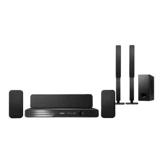
Dvd home theater system
Hide thumbs
Also See for HTS3367/12:
- Quick start manual (2 pages) ,
- Quick start manual (57 pages) ,
- Specifications (3 pages)
Table of Contents
Advertisement
Quick Links
DVD Home Theater System
Service
Service Manual
©
Copyright 2008 Philips Consumer Electronics B.V. Eindhoven, The Netherlands
All rights reserved. No part of this publication may be reproduced, stored in a retrieval system or
transmitted, in any form or by any means, electronic, mechanical, photocopying, or otherwise
without the prior permission of Philips.
Published by
LM0807
Service Audio Printed in The Netherlands Subject to modification
Version 1.0
TABLE OF CONTENTS
Location of PCB Boards ............................................. 1-2
Versions Variation ....................................................... 1-2
Specifications .............................................................. 1-3
Measurement Setup ....................................................1-4
Service Aids ................................................................ 1-5
ESD & Safety Instruction ............................................ 1-6
Lead-free solding Information .................................... 1-7
Setting procedure &Repair Instructions ......................... 2
Disassembly Instructions & Service positions .............. 3
Block & Wiring Diagram ................................................ 4
VFD+JACK+VOL+STANDBY Board .............................5
Main Board .....................................................................6
Power Board ...................................................................7
AMP Board .....................................................................8
Scart Board......................................................................9
Mechanical Exploded View & Parts...............................10
Revision list....................................................................11
1 - 1
Chapter
HTS3367
/12/05
GB
3139 785 33520
Advertisement
Table of Contents

Related Manuals for Philips HTS3367/12


Summary of Contents for Philips HTS3367/12
- Page 1 Revision list..............11 © Copyright 2008 Philips Consumer Electronics B.V. Eindhoven, The Netherlands All rights reserved. No part of this publication may be reproduced, stored in a retrieval system or transmitted, in any form or by any means, electronic, mechanical, photocopying, or otherwise without the prior permission of Philips.
-
Page 2: Location Of Pcb Boards
1 - 2 LOCATION OF PCB BOARDS SCART PCB MAIN PCB AMP PCB STANDBY PCB VFD PCB POWER PCB VOL PCB JACK PCB VERSION VARIATION: HTS3367 Type/Versions Features Main (Output Power-600W) S-Video Out Power Voltage (230V) Power Cord ( fixed ) SERVICE SCNARIO MATRIX: HTS3367 Type/Versions... -
Page 3: Specifications
1 - 3 SPECIFICATIONS MAIN UNIT AMPLIFIER Power Supply Rating: ........220 - 240V; 50Hz Total output power : Power Consumption: ............100 W - Home Theatre mode: ........... 600 W Dimensions: ..........435 x 57 x 360 (mm) Frequency Response: ...... 180 Hz – 18 kHz / ±3 dB ...................(w x h x d) Signal-to-Noise Ratio: ...... - Page 4 1 - 4 MEASUREMENT SETUP Tuner FM Bandpass LF Voltmeter 250Hz-15kHz e.g. PM2534 e.g. 7122 707 48001 RF Generator e.g. PM5326 S/N and distortion meter e.g. Sound Technology ST1700B Use a bandpass filter to eliminate hum (50Hz, 100Hz) and disturbance from the pilottone (19kHz, 38kHz). Use Audio Signal Disc SBC429 4822 397 30184 (replaces test disc 3)
- Page 5 1 - 5...
- Page 6 1 - 6...
- Page 7 1 - 7...
- Page 8 In open model, press “1“ “5“ “9“ on R/C the sofeware upgrade? b) press “ok” button to con rm c) TV will show message as below: Cancel Current model HTS3367/12 Version: 00.12.01_1 Release: 2007.12.19 f) select “OK”, OSD will show: Region Servo: 5B.61.00.00 8032: 05.00.04.06...
- Page 9 2 - 2 2 - 2 REPAIR INSTRUCTIONS (part one)
- Page 10 2 - 3 2 - 3 REPAIR INSTRUCTIONS (part two)
- Page 11 2 - 4 2 - 4 REPAIR INSTRUCTIONS (part three)
- Page 12 3 - 1 3 - 1 DISASSEMBLY INSTRUCTIONS Dismantling of the Front Panel Assemble 3) Loosen 7 screws and remove the Top Cover by lifting the rear portion upwards before sliding it out towards the rear. - 1 screw “A” each on the left & right side as shown in gure 4 1) Open the DVD Tray by using the Open/Close Button while the Set is ON and disconnect the mains supply after removing the Tray - 5 screws “B”...
- Page 13 3 - 2 3 - 2 Dismantling of the Main Board Dismantling of the Scart Board 1) Loosen 2 screws “ F “ on the top of main board as shown in gure 9 1) Loosen 2 screws “I” at the back panel as shown in gure 12 2) Loosen 7 screws “G”...
- Page 14 3 - 3 3 - 3 Dismantling of the DVD Module 1) Loosen 4 screws “L” as shown in gure 15. Figure 15 SERVICE POSITIONS Service position A (main unit) Figure 1 Note:In some service positions the components or copper patterns of one board may risk touching its neighbouring pc boards or metallic parts.
- Page 15 4 - 1 4 - 1 BLOCK DIAGRAM...
- Page 16 4 - 2 4 - 2 WIRING DIAGRAM...
- Page 17 5 - 1 5 - 1 FTD DISPLAY PIN ASSIGNMENT CONTROL BOARD TABLE OF CONTENTS FTD Display Pin Assignment ............. 5-1 Circuit Diagram ................. 5-2 PCB Layout Top & Bottom View ............5-3 PIN CONNECTION...
- Page 18 5 - 2 5 - 2 CIRCUIT DIAGRAM FB12 D3 LD11 A2 RB12 B1 SN11 B1 TA18 D2 FB13 D3 RB13 A1 TA11 C1 TA20 C2 FB14 D3 RB14 A1 TA12 C1 USB11 D3 FB15 D3 RB15 D3 TA13 D1 VR11 D4 DP11 A3 IC11...
- Page 19 5 - 3 5 - 3 PCB LAYOUT - TOP VIEW LD11 A1 RB12 A1 RB16 A4 TA12 A1 TA18 A4 RB13 A2 RB17 A3 TA13 A4 TA20 A3 DP11 A2 RB14 A1 SN11 A1 TA14 A1 USB11 A4 JK11 A4 RB11 A1 RB15 A4 TA11 A4...
-
Page 20: Main Board
6 - 1 6 - 1 INTERNAL IC DIAGRAM - AS81F641642C MAIN BOARD TABLE OF CONTENTS Internal IC Diagram ................6-1 Circuit Diagram (part one) ..............6-2 INTERNAL IC DIAGRAM - MT1389E Circuit Diagram (part two) ..............6-3 PCB Layout Top View ..............6-4 PCB Layout Bottom View .............. - Page 21 6 - 2 6 - 2 CIRCUIT DIAGRAM - part one C301 C920 FE309 D4 R353 C302 C921 FE310 D4 R354 C303 C922 FE311 D4 R355 C304 C923 FE312 D4 R356 C305 C924 IC301 A2 R357 C306 C928 IC302 A2 R358 C307 C929...
- Page 22 6 - 3 6 - 3 CIRCUIT DIAGRAM - part two C0201 C2 C224 C827 FB218 C1 Q720 R603 C0202 A3 C225 C828 FB219 C1 Q721 R604 C0203 A3 C226 C829 FB220 C1 Q801 R605 C0204 D1 C227 C830 FB221 C1 Q802 R606 C0205 A3...
- Page 23 6 - 4 6 - 4 PCB LAYOUT - TOP VIEW C0202 A3 C601 CN205 C3 L201 R248 R530 C0207 C2 C602 CN206 C5 L202 R249 R531 C0208 C3 C701 CN207 C4 L203 R250 R532 C0235 B3 C703 CN208 C3 L204 R251 R533...
- Page 24 6 - 5 6 - 5 PCB LAYOUT - BOTTOM VIEW C0201 B4 C518 CE316 A1 R388 C0203 B4 C519 CE317 A2 R399 C0204 B4 C520 CE318 A2 R601 C0205 C5 C521 CE319 B1 R606 C0206 B5 C600 CE320 B1 R722 C0209 B4 C603...
-
Page 25: Internal Ic Diagram
7 - 1 7 - 1 INTERNAL IC DIAGRAM - AP3843GMTR UVLO 2.50V INTERNAL BIAS VREF GOOD OUTPUT LOGIC POWER BOARD OVER TEMP PROTECT ERROR COMP LATCH CURRENT SENSE COMPARATOR TABLE OF CONTENTS Internal IC Diagram ................7-1 Circuit Diagram .................. 7-2 PCB Layout Top View ............... - Page 26 7 - 2 7 - 2 CIRCUIT DIAGRAM BD901 A1 C916 C929 C943 C956 C964C C1 C991 D909 D922 IC905 Q905 R9001 B1 R912 R926C A4 R941 R957 R970 R986 T901 ZD908 B4 C901 C917 C930 C944 C957 C966 CN903 A4 D910 D923 J903...
- Page 27 7 - 3 7 - 3 PCB LAYOUT - TOP VIEW BD901 C921 C945 C960 C971 CN908 D921 GT903 J911 J920 J929 L902 Q905 Q916 R936 R945 R969 T903 C901 C922 C946 C961 C977 D904 D922 IC901 J912 J921 J930 L903 Q909 R903...
- Page 28 7 - 4 7 - 4 PCB LAYOUT - BOTTOM VIEW C904 C919 C929 C942 C958A B2 C972 D908 IC902 C3 R902 R921 R926C B1 R944 R959 R973 R982 R993 ZD909 C3 C906 C923 C930 C946 C959 C973 D909 Q906 R910 R922 R926D B1...
-
Page 29: Amp Board
8 - 1 8 - 1 INTERNAL IC DIAGRAM - STA309A OUT1A/B LRCKI OUT2A/B BICKI SERIAL OVERSAMPING OUT3A/B SDI12 DATA OUT4A/B SDI34 SYSTEM OUT5A/B CONTROL SDI56 OUT6A/B SKI78 OUT7A/B AMP BOARD OUT8A/B VARIABLE TREBLE VOLUME CHANNEL OVER- BASS EQ LRCKO LIMITING MAPPING SAMPLING... -
Page 30: Circuit Diagram
8 - 2 8 - 2 CIRCUIT DIAGRAM C413 C435 C451 C471 C491 C505 C526 C542 CE411 C3 D411 JK401 A2 Q405 R413 R440 R456 R475 R491 R505 R522 R604 C414 C436 C452 C472 C492 C506 C528 C545 CE412 C3 D412 JK401A A2 Q406... -
Page 31: Pcb Layout Top View
8 - 3 8 - 3 PCB LAYOUT - TOP VIEW C507 C1 Q404 B1 R497 C1 C425 D3 C508 B1 Q407 C1 R498 C1 C425A D4 C513 A1 Q408 B1 R499 C1 C426 C4 C518 D1 Q409 B1 R500 C1 C427 C3 C519 D1 Q410 B1... -
Page 32: Pcb Layout Bottom View
8 - 4 8 - 4 PCB LAYOUT - BOTTOM VIEW D404 R507 C401 D405 R509 C402 D408 R510 C403 D410 R515 C404 D411 R522 C405 D412 R526 C406 D413 R527 C407 D414 R528 C408 D415 R529 C409 D416 R530 C410 R531 C411... -
Page 33: Scart Board
9 - 1 9 - 1 SCART BOARD TABLE OF CONTENTS Circuit Diagram ................. 9-2 PCB Layout View ................9-3... - Page 34 9 - 2 9 - 2 CIRCUIT DIAGRAM C710 A1 C711 A1 C712 C2 C713 B2 C714 B2 C715 A2 FB707 B2 FB708 B2 FB709 B2 FB710 A2 FB711 A2 FB714 C2 JK703 A2 R707 A2 R708 A2 RB701 B1 RB702 A3...
- Page 35 9 - 3 9 - 3 PCB LAYOUT - TOP VIEW C710 C711 C712 C713 C714 C715 FB707 B2 FB708 B2 FB709 B3 FB710 B1 FB711 B1 FB714 B3 JK703 A2 R707 R708 RB701 B3 RB702 B1...
- Page 36 10 - 1 10 - 1 MECHANICAL EXPLODED VIEW NOTE: A1=13+14+34+36...
- Page 37 10 - 2 10 - 2 MECHANICAL PART LIST Loc. 12NC. Description 996510010841 DISPLAY LENS 996510010839 USB DOOR LENS 996510010835 SOURCE BUTTON PC PMMA 996510010833 VOLUME KNOB PMMA PC 996510010832 FUNCTION BUTTON 996510010829 USB DOOR 996510012215 FRONT PANEL 996510010837 FUNCTION BRACKET 996510010834 EJECT KEY 996510012214...
-
Page 38: Revision List
11 - 1 11 - 1 REVISION LIST Version 1.0 *Initial release...