Yamaha DME 32 Service Manual
Hide thumbs
Also See for DME 32:
- Owner's manual (296 pages) ,
- Owner's manual (16 pages) ,
- Hardware setup manual (12 pages)
Table of Contents
Advertisement
Quick Links
This document is printed on chlorine free (ECF) paper with soy ink.
PA
011522
200007**
DIGITAL MIXING ENGINE
SERVICE MANUAL
CONTENTS
SPECIFICATIONS ···································································· 3
PANEL LAYOUT······································································· 5
CIRCUIT BOARD LAYOUT ······················································ 7
DIMENTIONS ··········································································· 8
DISASSEMBLY PROCEDURE················································· 9
LSI PIN DESCRIPTION ·························································· 12
IC BLOCK DIAGRAM ····························································· 19
TEST PROGRAM AND INSPECTION···································· 22
FLASH ROM UPGRADE ························································ 27
ERROR MESSAGES······························································ 28
MIDI IMPLEMENTATION CHART ·········································· 31
MIDI DATA FORMAT······························································ 32
CIRCUIT BOARDS ································································· 34
PARTS LIST
CIRCUIT DIAGRAM AND BLOCK DIAGRAM
HAMAMATSU, JAPAN
1.44K-6661 K
Printed in Japan '00.08
Advertisement
Table of Contents

Related Manuals for Yamaha DME 32


Summary of Contents for Yamaha DME 32
- Page 1 DIGITAL MIXING ENGINE SERVICE MANUAL CONTENTS SPECIFICATIONS ···································································· 3 PANEL LAYOUT······································································· 5 CIRCUIT BOARD LAYOUT ······················································ 7 DIMENTIONS ··········································································· 8 DISASSEMBLY PROCEDURE················································· 9 LSI PIN DESCRIPTION ·························································· 12 IC BLOCK DIAGRAM ····························································· 19 TEST PROGRAM AND INSPECTION···································· 22 FLASH ROM UPGRADE ························································ 27 ERROR MESSAGES······························································...
-
Page 2: Specifications
IMPORTANT NOTICE This manual has been provided for the use of authorized Yamaha Retailers and their service personnel. It has been assumed that basic service procedures inherent to the industry, and more specifically Yamaha Products, are already known and understood by the users, and have therefore not been restated. - Page 3 DME32 SPECIFICATIONS Internal 48 kHz Sampling frequency External 39.69–50.88 kHz Signal delay 0.21 ms (direct cable from input 1 to output 1, fs = 48 kHz) Configuration 2 (A, B) Memories Scene 99 per configuration Display 24-character x 2 line LCD, with backlight Scene No.
-
Page 4: Connector Pin Assignments
DME32 Connector Pin Assignments PC CONTROL (RS232C) Name In/Out Name In/Out Unused — Unused — — PC CONTROL (RS422) Name In/Out Name In/Out Unused — Unused — — CASCADE OUT CASCADE IN Name Name Name Name Bus 1–4 in+ Bus 1–4 in- Bus 1–4 out+ Bus 1–4 out- Bus 5–8 in+... -
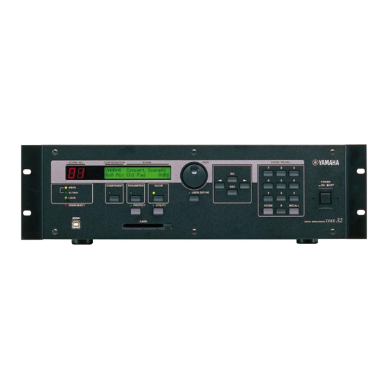
Page 5: Panel Layout
DME32 PANEL LAYOUT Front Panel 9 10 11 12 13 14 15 17 18 19 20 SCENE NO. indicator Scene edit dots Display DATA wheel INC & DEC buttons STORE button SCENE RECALL number keypad RECALL button 48kHz & 44.1kHz indicators LOCK indicator EMERGENCY indicator USB port... - Page 6 DME32 Rear Panel 25 26 AC IN connector WORD CLOCK OUT connector WORD CLOCK 75 ohm ON/OFF switch WORD CLOCK IN connector MIDI IN & OUT ports PC CONTROL RS232C/RS422 switch PC CONTROL port COM port CASCADE OUT port CASCADE IN port Ground terminal GPI connectors SLOTs 1–4...
-
Page 7: Circuit Board Layout
DME32 CIRCUIT BOARD LAYOUT MAIN 3/3(GPI) CN016 Power Supply Unit (MYMB) CN012 CN004 CN014 CN006 CN013 CN018 CN010 CN011 CN017 CN008 CN005 CN007 CN502 CN501 3/4(LED) 2/4(ENC) 2/3(PCMUSB) 1/4(FP) 4/4(PSW) -
Page 8: Dimentions
DME32 DIMENTIONS W: 480 H: 141.5 Unit: mm... -
Page 9: Disassembly Procedure
DME32 DISASSEMBLY PROCEDURE Top Cover Remove the fourteen (14) screws marked [470]. The top cover can then be removed. (Fig. 1) Front Panel Assembly Remove the top cover. (See procedure 1.) Remove the six (6) screws marked [350]. The left and right mount brackets can then be removed. - Page 10 DME32 <Rear View> [420] [430] [290]: Pan Head Screw 2.6X6 MFZN2BL (VC990500) [420]: Bonding Screw 3.0X6 MFZN2BL (VS863000) [430]: Bonding Tapping Screw-B 3.0X8 MFZN2BL (VN413300) [290] 3/3(GPI) [290] Fig. 3 <Top View> • Lithium Battery Battery VN103500 MAIN [150] VN103600(Battery holder for VN103500) [440] Notice for back-up battery removal Battery...
- Page 11 DME32 PNF1/4(FP) Circuit Board: Remove the four (4) screws marked [30A]. The PNF1/4(FP) circuit board can then be removed. (Fig. 7) PNF2/4(ENC) Circuit Board: Remove the four (4) screws marked [30B]. The PNF2/4(ENC) circuit board can then be removed. And then pull out the encoder knob from the PNF2/4(ENC) circuit board.
-
Page 12: Lsi Pin Description
DME32 LSI PIN DESCRIPTION HD6437042AF62F (XY885B00) CPU ································································································· 14 MR-SHPC-01 (XW937A00) PC Card Controller ················································································ 15 SGH609080F-47F (XU235A00) ATSC ································································································ 16 YSS904-F (XV989A00) DSP5 (Digital Signal Processor)····································································· 17 YSS910-S (XV988A00) DSP6 (Digital Signal Processor) ···································································· 18 PDIUSBD12PW (XW583A00) USB Interface······················································································ 19 ST16C554DCQ64 (XW934A00) UART (Universal Asynchronous Receiver and Transmitter) ············... - Page 13 DME32 MR-SHPC-01 (XW937A00) PC Card Controller PNR: IC101 NAME FUNCTION NAME FUNCTION Ground Ground /RESET System reset Card data bus /SRD Read command CD10 /SWE0 CWP XIOIS16 Write protect / 16 bit cycle request Write command /SWE1 /CCD2 Card detect Bus strobe CVPP1 Card slot power supply...
- Page 14 DME32 SGH609080F-47F (XU235A00) ATSC MAIN: IC38, 42 NAME FUNCTION NAME FUNCTION syncati Synch. word input terminal for ati, synci Synch. word input terminal for si3-0 input siat3-0 input mccti 64 fs clock input terminal for ati, mcci 64 fs clock input terminal for si3-0 input siat3-0 input mcbti 128 fs clock input terminal for ati,...
- Page 15 DME32 YSS904-F (XV989A00) DSP5 (Digital Signal Processor) MAIN: IC106, 107, 110 NAME FUNCTION NAME FUNCTION Not used Not used Ground SIO28 Power supply SIO29 Serial data bus System master clock input (60 MHz or 30 MHz) SIO30 System master clock output (High or 30 MHz) SIO31 Ground Power supply...
- Page 16 DME32 YSS910-S (XV988A00) DSP6 (Digital Signal Processor) MAIN: IC77, 80, 83, 86, 89, 92, 95, 98, 101, 104 NAME FUNCTION NAME FUNCTION Power supply (3.3 V) Ground Ground DB13 System master clock input (60 MHz or 30 MHz) DB14 System master clock output (High or 30 MHz) DB15 Power supply (5 V) DB16...
- Page 17 DME32 PDIUSBD12PW (XW583A00) USB Interface PNR: IC102 NAME FUNCTION NAME FUNCTION DATA0 Bit 0 of bi-directional data. RD_N Read Strobe (Active Low) DATA1 Bit 1 of bi-directional data. WR_N Write Strobe (Active Low) DATA2 Bit 2 of bi-directional data. DMREQ DMA Request.
- Page 18 DME32 TPS2205IDB (XW602A00) Power Controller PNR: IC104 NAME FUNCTION NAME FUNCTION Card power (5 V) 3.3V Card power (3.3 V) Card power (5 V) 3.3V Card power (3.3 V) A_PGM AVPP voltage control Overflow control ("L" level signal output) A_Vcc AVPP voltage control Not used /A_Vcc...
-
Page 19: Ic Block Diagram
DME32 IC BLOCK DIAGRAM MM74HCU04SJX (XY070A00) MM74HC14SJX (XW104A00) 74VHC32SJX (XY306A00) TC74HC04AF (XS993A00) Hex Inverter Quad 2 Input OR HD74LVC04FP (XW905A00) MAIN: IC19 MAIN: IC3, 5 Hex Inverter MAIN: IC16, 25 PNR: IC103 MM74HC74ASJX (XY153A00) TC74HC123AF (XN242A00) TC74VHC138F (XT015A00) Dual D-Type Flip-Flop Dual Retriggerable Single Shot 3 to 8 Demultiplexer MAIN: IC17, 22... - Page 20 DME32 MM74HC175SJX (XY307A00) MM74HC245ASJX (XW107A00) MM74HC273SJX (XY198A00) Quad D-Type Flip-Flop SN74ABT245BNSR (XU009A00) Octal D-Type Flir Flop TC74VHC245F (XT487A00) MAIN: IC24, 46-49 MAIN: IC23 Octal 3-State Bus Transceiver MAIN: IC29-31, 50-52, 60, 61, 66-75 CLEAR Q CL D CK Q CL D CK CLOCK TC74HC4052AF (XS790A00)
- Page 21 DME32 DS26C32ATMX (XU815A00) NJM2082M-T1 (XN797A00) Quad Differential Line Receiver Dual Operational Amplifier MAIN: IC32, 33, 120, 121 MAIN: IC1 +DC Voltage INPUT A Output A Supply Inverting INPUT A INPUT B Output B Input A Inverting Non-Inverting OUTPUT A INPUT B Input B Input A Non-Inverting...
-
Page 22: Test Program
DME32 TEST PROGRAM AND INSPECTION Preparation Note:cont.dll cont.dll is not included in the master data that has been 1-1. Initial settings attached. Copy it from C:¥Program Files¥Dme that DME • Connect the [CASCADE IN] terminal and [CASCADE OUT] Manager has installed. terminal with a SCSI 50p cable. - Page 23 DME32 Click [NEXT] and check boxes are set to on and the inspection goes to the next item. Use the following buttons as needed. Click [END] to end the test program. The screen returns to the 2-2-5. Word Clock one shown in “2-2-1 Selecting the main sheet inspection items”. Click [ABORT] to interrupt the diagnosis.
- Page 24 DME32 (1) DSP6 Displays the results of a circuit check from the So terminal of DSP6 to the Si terminal of DSP6 via DSP5. (2) DRAM Tx-Rx: Communication circuit check. Displays the results of the DRAM address bus and data bus D0-D7: Data bus check.
- Page 25 DME32 2-3-6. SWITCH Press the switches in the sequence indicated and the results of the diagnosis will be shown. 2-3-10. USB 2-3-7. DATA ENCODER Turn [DATA] knob in the direction indicated and the results of Follow the instructions and connect the USB terminal of the PC the diagnosis will be shown.
-
Page 26: Factory Settings
DME32 • Select Data Transfer Menu and then “A” from the list. The WORD CLOCK Permissible Range LED ON Check name will change in the title column. Click [Execute]. A 44.1 kHz 5 nSec or less 44.1 kHz/LOCK confirmation message will be displayed. Click [OK]. 48 kHz 5 nSec or less 48 kHz/LOCK... - Page 27 DME32 FLASH ROM UPGRADE 1. Turn on the power with press and hold [STORE] and [0] keys on DME32. LCD Display on DME32. System prog Ver.00.07 Install All Ready 2. Press [RECALL] key on DME32. System prog Ver.00.07 Flash-R Erasing Now... Then, wait until display showing the following.
-
Page 28: Error Messages
DME32 ERROR MESSAGE If the DME32 displays an error message, look for the solution in the following table. Message Reason Solution ****** WARNING ****** The internal battery has expired. Save the configurations to DME Man-ager or a PC Card, LOW BATTERY and then replace the battery. - Page 29 DME32 DME Manager Error Messages If DME Manager displays an error message, look for the solution in the following table. Message Reason Solution Cannot compile because An attempt was made to compile a configuration that Add some components, and then try compiling again. configuration contains no contains no components.
- Page 30 DME32 Message Reason Solution This operation is protected! An attempt was made to use a protected operation. Turn off the Operation or Component protection, and then try again. Too many components for The maximum number of components for the speci- Delete any unused components in order to free up resourc- DME32 #! fied DME32 has been exceeded.
-
Page 31: Midi Implementation Chart
DME32 MIDI IMPLEMENTATION CHART YAMAHA [Digital Mixing Engine] Date: 1 May 2000 MIDI Implementation Chart Model: DME32 Version: 1.0 Function... Transmitted Recognized Remarks Basic Default 1–16 1–16 Memorized Channel Changed 1–16 1–16 Default OMNI OFF/OMNI ON Mode Messages Memorized Altered... -
Page 32: Midi Data Format
DME32 MIDI Data Format 1. Transmit/Receive Data 3. MIDI Format Table 1.1 Program Change 3.1 Channel Message When a Program Change message is received, the scene specified in the [ Program Change Assign Table ] is recalled. Command rx/tx Function Program Change messages are transmitted according to the [ Program Bn Control Change rx/tx... - Page 33 These messages are transmitted without change if [Parameter Change ECHO] is ON. STATUS 11110000 F0 System Exclusive Message Manufacturer's ID No. ( YAMAHA ) ID No. 01000011 43 SUB STATUS 0001nnnn 1n parameter change or response for request n=0-15 ( Device Channel No.1-16 )
-
Page 34: Circuit Boards
DME32 CIRCUIT BOARDS PNR1/3 ( MYMB ) Circuit Board PNR2/3 ( PCMUSB ) Circuit Board to MAIN -CN017 to MAIN -CN018 SLOT 1 SLOT 2 to MAIN -CN011 Power supply unit -CN4 to MAIN -CN013 to MAIN -CN014 SLOT 3 SLOT 4 to MAIN -CN012 Component side... -
Page 35: Parts List
DME32 MAIN Circuit Board WORD CLOCK PC CONTROL MIDI CASCADE IN CASCADE OUT to Power supply unit-CN5 • Lithium Battery Battery VN103500 VN103600(Battery holder for VN103500) Notice for back-up battery removal Battery Push the battery as shown in figure, then the battery will pop up. Druk de batterij naar beneden zoals aangeven in de tekening, de batterij springt dan naar voren. -
Page 36: Parts List
DME32 MAIN Circuit Board Pattern side Note: See parts list for details of circuit board component parts. 3NA-V512930-3... -
Page 37: Parts List
DME32 PNF1/4 ( FP ) Circuit Board to MAIN-CN006 to MAIN-CN004 48KHz 44.1KHz COMPPONENT PARAMETER VALUE USER DEFINE LOCK EMERGENCY STORE RECALL PROTECT UTILITY Component side Pattern side PNF2/4 ( ENC ) Circuit Board PNF3/4 ( LED ) Circuit Board PNF4/4 ( PSW ) Circuit Board to MAIN-CN007 to MAIN-CN005... -
Page 38: Parts List
DIGITAL MIXING ENGINE PARTS LIST CONTENTS OVERALL ASSEMBLY······························································································································ 2 FRONT PANEL ASSEMBLY ····················································································································· 5 ELECTRICAL PARTS ························································································································· 6~12 Notes: DESTINATION ABBREVIATIONS Australian model M: South African model British model Chinese model Canadian model South-east Asia model German model Taiwan model European model U.S.A. - Page 39 DME32 OVERALL ASSEMBLY Rear panel assembly 40ba 360a 360c H, W, B, V J, U 360b Bottom assembly Front panel assembly:See page 5.
- Page 40 DME32 PART NO. DESCRIPTION REMARKS REF NO. RANK OVERALL ASSEMBLY DME32 Overall Assembly (V520670) Overall Assembly (V520680) Overall Assembly H,W,B,V (V580010) Bottom Assembly (V593160) V5202700 Bottom Chassis CB806590 VR138400 Bind Head Tapping Screw-B 4.0X12 MFZN2BL Protection Sheet (V520520) Label CAUTION U,H,W,B,V (V533520) Label...
- Page 41 DME32 PART NO. DESCRIPTION REMARKS REF NO. RANK VN413300 Bonding Tapping Screw-B 3.0X8 MFZN2BL EP600230 Bind Head Tapping Screw-B 3.0X6 MFZN2BL VN103500 Lithium Battery CR2032 V5202400 Top Cover VC688800 Bind Head Tapping Screw-B A4.0X8 MFZN2BL VZ678500 IF Plate VP156900 Bind Head Screw A4.0X12 MFZN2BL Label, Date Cord (VA03930)
- Page 42 DME32 FRONT PANEL ASSEMBLY PART NO. DESCRIPTION REMARKS REF NO. RANK FRONT PANEL ASSEMBLY DME32 Front Panel Assembly (V529550) V5203800 Sub Chassis Circuit Board (V512940) AAX13980 Circuit Board PNF 1/4 (FP) AAX13990 Circuit Board PNF 2/4 (ENC) AAX14000 Circuit Board PNF 3/4 (LED) AAX14010 Circuit Board...
- Page 43 DME32 ELECTRICAL PARTS PART NO. DESCRIPTION REMARKS REF NO. RANK ELECTRICAL PARTS DME32 V5129300 Circuit Board MAIN (XW953B0) Circuit Board (V512940,XY041B0) AAX13980 Circuit Board PNF 1/4 (FP) (XY041B0) AAX13990 Circuit Board PNF 2/4 (ENC) (XY041B0) AAX14000 Circuit Board PNF 3/4 (LED) (XY041B0) AAX14010 Circuit Board...
-
Page 44: Table Of Contents
DME32 PART NO. DESCRIPTION REMARKS REF NO. RANK VK025300 Wire Trap 52147 9P TE VK024700 Wire Trap 52147 3P TE VP214600 Header, Flat Cable HIF3FC 16P TE V4795900 Connector, FCN-235D 230R(IPI) 50P SE CASCADE OUT CN10 VQ048500 Connector, FFC 52045 36P TE VQ048500 Connector, FFC 52045 36P TE... - Page 45 DME32 PART NO. DESCRIPTION REMARKS REF NO. RANK IC52 XW107A00 MM74HC245ASJX TRANSCEIVER IC60 XW107A00 MM74HC245ASJX TRANSCEIVER IC61 XW107A00 MM74HC245ASJX TRANSCEIVER IC62 XY308A00 MM74HC151SJX DATA SELECTOR IC63 XY308A00 MM74HC151SJX DATA SELECTOR IC64 XT015A00 TC74VHC138F DECODER IC65 XT015A00 TC74VHC138F DECODER IC66 XT487A00 TC74VHC245F TRANSCEIVER IC67...
- Page 46 DME32 PART NO. DESCRIPTION REMARKS REF NO. RANK V5477300 LED (chip) CL-190R-CD-T RE RD257100 Carbon Resistor (chip) 10.0K 0.1 J RD259470 Carbon Resistor (chip) 4.7M 0.1 J RD256300 Carbon Resistor (chip) 3.0K 0.1 J RD255220 Carbon Resistor (chip) 220.0 0.1 J RD257100 Carbon Resistor (chip) 10.0K 0.1 J...
- Page 47 DME32 PART NO. DESCRIPTION REMARKS REF NO. RANK -133 RD256220 Carbon Resistor (chip) 2.2K 0.1 J R134 RD257100 Carbon Resistor (chip) 10.0K 0.1 J -140 RD257100 Carbon Resistor (chip) 10.0K 0.1 J R141 RD255150 Carbon Resistor (chip) 150.0 0.1 J -148 RD255150 Carbon Resistor (chip)
- Page 48 DME32 PART NO. DESCRIPTION REMARKS REF NO. RANK Circuit Board (V515960,XY231B0) AAX13970 Circuit Board PNR 1/3 (MYMB) (XY231B0) AAX13950 Circuit Board PNR 2/3 (PCMUSB) (XY231B0) AAX13960 Circuit Board PNR 3/3 (GPI) (XY231B0) VB659000 Bind Head Screw 3.0X8 MFZN2BL V5782900 Bind Head Screw 2.0X8 MFZN2BL ES200030 Hexagonal Nut...
- Page 49 DME32 PART NO. DESCRIPTION REMARKS REF NO. RANK V5149400 LCD Assembly 24X2 CONFIGURATION-SCENE V5065200 AC Inlet M1908-C 3P AC IN VN103500 Lithium Battery CR2032 V5436200 Cable, D-Sub 17JE 414 9P VN580000 AC Cord DC-015-J01 2.5m VB506800 AC Cord VB928000 AC Cord V6190800 AC Cord BS 3P...
-
Page 50: Parts List
DIGITAL MIXING ENGINE CIRCUIT DIAGRAM CONTENTS BLOCK DIAGRAM ················································································································ 3 WIRING ································································································································· 5 MAIN CIRCUIT DIAGRAM ···································································································· 6 PNF CIRCUIT DIAGRAM ···································································································· 25 PNR 2/3 ( PCMUSB ) CIRCUIT DIAGRAM ( PNR 2/3 ( PCMUSB ) ········································· 26 PNR 1/3 ( MYMB ) CIRCUIT DIAGRAM ( PNR 1/3 ( MYMB ) ·················································· 27 PNR 3/3 ( GPI ) CIRCUIT DIAGRAM ( PNR 3/3 ( GPI ) ···························································... - Page 51 BLOCK DIAGRAM 002 ( DME32 ) DME32 CPU BUS FPGA BUS PCMUSB CARD X101 6MHz CARD I/F Power USB I/F Controller IC101 IC102 IC104 176p A[12-14] Selector /D6WAIT[1-8] Driver Driver IC062 /DSPWAIT1 Receiver Receiver p.11 Receiver flash memory SRAM SRAM SRAM SRAM SRAM...
- Page 52 BLOCK DIAGRAM 003 ( DME32 ) DME32 CPU BUS FPGA BUS /RESET[2] MYTX,MYRX /RST1 /WR1 /RD1 Driver X004 /SYNCO,CKO IC074 p.17 Transceiver Transceiver Transceiver Transceiver Transceiver Transceiver 60MHz IC075 IC052 20p IC053 IC054 IC055 IC056 IC057 D51S[48-51] p.12 SYNCI[3],CKI[3] p.10 p.10 p.10 p.10...
- Page 53 WIRING ( DME32 ) DME32 ( MYMB ) MAIN ( PCMUSB ) ( FP ) ( GPI ) ( LED ) ( ENC ) LCD Ass'y (V514940) LCD DISPLAY POWER SUPPLY Primary Secondary ( PSW ) WIRING ( DME32 ) KEC-92548...
-
Page 54: Op Amp
MAIN CIRCUIT DIAGRAM 002 ( DME32 ) DME32 OP AMP SYSTEM RESET OP AMP : Ceramic Capacitor MAIN CIRCUIT DIAGRAM 002 ( DME32 ) KEC-92549-002... -
Page 55: Flash Rom 8M
MAIN CIRCUIT DIAGRAM 003 ( DME32 ) DME32 FLASH ROM 8M SRAM 1M SRAM 1M SRAM 1M SRAM 1M SRAM 1M SRAM 1M SRAM 1M SRAM 1M : Ceramic Capacitor MAIN CIRCUIT DIAGRAM 003 ( DME32 ) KEC-92549-003... -
Page 56: Fpga
MAIN CIRCUIT DIAGRAM 004 ( DME32 ) DME32 FPGA : Ceramic Capacitor MAIN CIRCUIT DIAGRAM 004 ( DME32 ) KEC-92549-004... -
Page 57: Inverter
MAIN CIRCUIT DIAGRAM 005 ( DME32 ) DME32 LINE DRIVER /RECEIVER UART INVERTER D-FF INVERTER D-FF INVERTER Photo Coupler INVERTER : Ceramic Capacitor MAIN CIRCUIT DIAGRAM 005 ( DME32 ) KEC-92549-005... -
Page 58: D-Ff
MAIN CIRCUIT DIAGRAM 006 ( DME32 ) DME32 DATA SELECTOR TRANSCEIVER DIR2 D-FF DATA SELECTOR D-FF D-FF to PNF 1/4 from PNF 1/4 (FP)-CN202 (FP)-CN201 TRANSCEIVER from PNF 2/4 (ENC)-CN301 to PNF 3/4 INVERTER (LED)-CN401 D-FF INVERTER TRANSCEIVER : Mylar Capacitor : Ceramic Capacitor : Metal Oxide Film Resistor MAIN CIRCUIT DIAGRAM 006 ( DME32 ) -
Page 59: Line Receiver
MAIN CIRCUIT DIAGRAM 007 ( DME32 ) DME32 LINE RECEIVER LINE RECEIVER LINE DRIVER LINE DRIVER /RECEIVER LINE DRIVER LINE DRIVER : Ceramic Capacitor MAIN CIRCUIT DIAGRAM 007 ( DME32 ) KEC-92549-007... -
Page 60: Atsc
MAIN CIRCUIT DIAGRAM 008 ( DME32 ) DME32 ATSC ATSC LINE DRIVER DIR2 LINE RECIEVER SINGLE SHOT INVERTER INVERTER : Mylar Capacitor : Ceramic Capacitor MAIN CIRCUIT DIAGRAM 008 ( DME32 ) KEC-92549-008... -
Page 61: Multiplexer
MAIN CIRCUIT DIAGRAM 009 ( DME32 ) DME32 D-FF TRANSCIEVER to PNR 3/3 (GPI)-CN701 MULTIPLEXER D-FF D-FF TRANSCIEVER MULTIPLEXER D-FF : Ceramic Capacitor MAIN CIRCUIT DIAGRAM 009 ( DME32 ) KEC-92549-009... - Page 62 MAIN CIRCUIT DIAGRAM 010 ( DME32 ) DME32 TRANSCIEVER to PNR 1/3 (MYMB)-CN607 to PNR 1/3 (MYMB)-CN605 TRANSCIEVER TRANSCIEVER TRANSCIEVER TRANSCIEVER TRANSCIEVER to PNR 1/3 (MYMB)-CN608 to PNR 1/3 TRANSCIEVER (MYMB)-CN606 TRANSCIEVER TRANSCIEVER TRANSCIEVER : Ceramic Capacitor MAIN CIRCUIT DIAGRAM 010 ( DME32 ) KEC-92549-010...
- Page 63 MAIN CIRCUIT DIAGRAM 011 ( DME32 ) DME32 TRANSCIEVER DATA SELECTOR TRANSCIEVER DATA SELECTOR DECORDER TRANSCIEVER DECORDER TRANSCIEVER TRANSCIEVER TRANSCIEVER TRANSCIEVER TRANSCIEVER : Ceramic Capacitor MAIN CIRCUIT DIAGRAM 011 ( DME32 ) KEC-92549-011...
- Page 64 MAIN CIRCUIT DIAGRAM 012 ( DME32 ) DME32 DRAM 16M DRAM 16M DRAM 16M DRAM 16M TRANSCIEVER DSP6 DSP6 TRANSCIEVER : Ceramic Capacitor MAIN CIRCUIT DIAGRAM 012 ( DME32 ) KEC-92549-012...
- Page 65 MAIN CIRCUIT DIAGRAM 013 ( DME32 ) DME32 DRAM 16M DRAM 16M DRAM 16M DRAM 16M DSP6 DSP6 : Ceramic Capacitor MAIN CIRCUIT DIAGRAM 013 ( DME32 ) KEC-92549-013...
- Page 66 MAIN CIRCUIT DIAGRAM 014 ( DME32 ) DME32 DRAM 16M DRAM 16M DRAM 16M DRAM 16M DSP6 DSP6 : Ceramic Capacitor MAIN CIRCUIT DIAGRAM 014 ( DME32 ) KEC-92549-014...
- Page 67 MAIN CIRCUIT DIAGRAM 015 ( DME32 ) DME32 DRAM 16M DRAM 16M DRAM 16M DRAM 16M DSP6 DSP6 : Ceramic Capacitor MAIN CIRCUIT DIAGRAM 015 ( DME32 ) KEC-92549-015...
- Page 68 MAIN CIRCUIT DIAGRAM 016 ( DME32 ) DME32 DRAM 16M DRAM 16M DRAM 16M DRAM 16M DSP6 DSP6 : Ceramic Capacitor MAIN CIRCUIT DIAGRAM 016 ( DME32 ) KEC-92549-016...
- Page 69 MAIN CIRCUIT DIAGRAM 017 ( DME32 ) DME32 DSP5 DSP5 MULTIPLEXER : Ceramic Capacitor MULTIPLEXER MAIN CIRCUIT DIAGRAM 017 ( DME32 ) KEC-92549-017...
- Page 70 MAIN CIRCUIT DIAGRAM 018 ( DME32 ) DME32 DSP5 : Ceramic Capacitor MAIN CIRCUIT DIAGRAM 018 ( DME32 ) KEC-92549-018...
- Page 71 MAIN CIRCUIT DIAGRAM 019 ( DME32 ) DME32 TRANSCIEVER TRANSCIEVER to PNR 2/3 (PCMUSB) - CN101 TRANSCIEVER TRANSCIEVER TRANSCIEVER TRANSCIEVER to PNR 2/3 (PCMUSB) - CN102 TRANSCIEVER from POWER SUPPLY UNIT - CN5 : Ceramic Capacitor MAIN CIRCUIT DIAGRAM 019 ( DME32 ) KEC-92549-019...
- Page 72 MAIN CIRCUIT DIAGRAM 020 ( DME32 ) DME32 LINE DRIVER LINE DRIVER LINE RECIEVER LINE RECIEVER LINE RECIEVER/DRIVER : Ceramic Capacitor MAIN CIRCUIT DIAGRAM 020 ( DME32 ) KEC-92549-020...
- Page 73 PNF CIRCUIT DIAGRAM ( DME32 ) DME32 1/4 FP to MAIN-CN006 to MAIN-CN004 2/4 ENC 3/4 LED 4/4 PSW to MAIN-CN005 to AC inlet to POWER SUPPLY UNIT - CN1 to MAIN-CN007 PNF CIRCUIT DIAGRAM ( DME32 ) KEC-92550...
- Page 74 PNR 2/3 ( PCMUSB ) CIRCUIT DIAGRAM 002 ( DME32 ) DME32 USB I/F to MAIN-CN017 INVERTER to MAIN-CN018 POWER CONNECTOR PC CARD CONTROLLER POWER CONTROLLER to POWER SUPPLY UNIT -CN4 : Ceramic Capacitor PNR 2/3 ( PCMUSB ) CIRCUIT DIAGRAM 002 ( DME32 ) KEC-92551-002...
- Page 75 PNR 1/3 ( MYMB ) CIRCUIT DIAGRAM 003 ( DME32 ) DME32 to MAIN-CN012 to MAIN-CN014 to MAIN-CN013 to MAIN-CN011 to POWER SUPPLY UNIT-CN2 PNR 1/3 ( MYMB ) CIRCUIT DIAGRAM 003 ( DME32 ) KEC-92551-003...
- Page 76 PNR 3/3 ( GPI ) CIRCUIT DIAGRAM 004 ( DME32 ) DME32 IN/+V SLOT 1-8 IN/+V SLOT 9-16 to MAIN-CN010 OUT/GND SLOT 1-8 OUT/GND SLOT 9-16 to POWER SUPPLY UNIT-CN3 PNR 3/3 ( GPI ) CIRCUIT DIAGRAM 004 ( DME32 ) KEC-92551-004...
- Page 77 POWER SUPPLY UNIT CIRCUIT DIAGRAM 1/3 ( DME32 ) DME32 2200P/250 NT-341F S2L60 1DL42A BL02-RN1 NL-112 1P220K 100/25 5D-11 HR-28-E253 HR-28-E253 S3L60 T2AH250V to PNF 4/4 2SK2028-01M 430V 0.47/250V 0.1/250 0.1/250 0.33/250 220K 2P1K (PSW) -CN501 5D-11 B2P3-VH-B D3SBA60 2SC4615E 2SK1982-01M 1GWJ43 100K...
- Page 78 POWER SUPPLY UNIT CIRCUIT DIAGRAM 2/3 ( DME32 ) DME32 NL-116 1SS133 BA17820T +20V BL02-RN1 GND(AG) 1GU42 GND(DG) NL-116 ICP-N50 1SS133 ICP-N50 BA17815T 0.1/50 0.1/50 to PNR 1/3 (MYMB) -CN609 BL02-RN1 D1NS6 -15V NL-116 -15V 1SS133 +15V ICP-N50 +15V 0.1/50 0.1/50 BA05T B13B-PH-K-S...
- Page 79 POWER SUPPLY UNIT CIRCUIT DIAGRAM 3/3 ( DME32 ) DME32 2SD1863R D101 Q101 1SS133 C102 T101 IC101E IC101A 0.1/50 TC4049BF TC4049BF NT-358 R102 R101 1K D102 CN100 MTZJ13B 1SS133 C101 Q102 100P/50 DRIVE 2SB1241R IC101C IC101D B3PS-BC-1 TC4049BF TC4049BF IC101B IC101F TC4049BF TC4049BF...