Advertisement
Table of Contents
- 1 Specification
- 2 Section 1 Precaution
- 3 Preventing Static Electricity
- 4 Important for Laser Products
- 5 Section 2 Specific Service Instructions
- 6 Section 3 Disassembly
- 7 Section 4 Adjustment
- 8 Test Mode
- 9 Operation
- 10 Power off
- 11 Display Content
- 12 Section 5 Troubleshooting
- 13 Schematic Diagrams
- 14 Parts List
- Download this manual
See also:
Instruction Manual
B53-0993-20
SERVICE MANUAL
10
2013
WA063<Rev.003>
DPX-U5130, DPX-U5130BT, DPX300U,
DPX305U, DPX405BT, DPX500BT,
DPX5130BTPT4, DPXU5130MM3
Mounting hardware assy
(J22-0429-23)
Compact disc
(W01-2054-05)
COPYRIGHT © 2013 JVC KENWOOD Corporation
B53-0993-20
SERVICE MANUAL
DUAL SIZED CD RECEIVER
DC cord
(E30-6939-05)
Screw set
(N99-18xx-05)
COPYRIGHT © 2013 JVC KENWOOD Corporation
DPX-U5130 (Korea)
DPX-U5130 (Other Areas)
DPX5130BTPT4 (TOYOTA in Philippines) : M3
DPXU5130MM3 (MITSUBISHI in Malaysia) : M4
DC cord
DC cord
(E30-6940-15)
(E30-8314-05)
Lever
Escutcheon
(D10-7012-04) x2
(B07-3379-02)
This product complies with the RoHS directive for the European market.
Microphone (3m)
Remote control unit
(QAN0126-001)
(RC-406)
(QAL1303-004)
Spacer (for old NISSAN)
Escutcheon
(J30-1106-04) x2
(B07-338x-01)
This product uses Lead Free solder.
No.WA063<Rev.003>
: H1
: M2
PbF
2013/10
Advertisement
Table of Contents

Related Manuals for Kenwood DPX-U5130


Summary of Contents for Kenwood DPX-U5130
- Page 1 (W01-2054-05) (N99-18xx-05) (D10-7012-04) x2 (J30-1106-04) x2 (B07-3379-02) (B07-338x-01) This product uses Lead Free solder. This product complies with the RoHS directive for the European market. COPYRIGHT © 2013 JVC KENWOOD Corporation B53-0993-20 No.WA063<Rev.003> COPYRIGHT © 2013 JVC KENWOOD Corporation 2013/10...
-
Page 2: Specification
SPECIFICATION Models for destination "K" (DPX300U, DPX500BT) FM tuner section Frequency range (200 kHz step) 87.9 - 107.9 MHz 9.3 dBf (0.8 µV/75 Ω) Usable sensitivity (S/N= 30 dB) 10.2 dBf (1.13 µV/75 Ω) Quieting sensitivity (DIN S/N = 46 dB) Frequency response (±... - Page 3 SPECIFICATION Models for destination "E" (DPX305U, DPX405BT) FM tuner section Frequency range (50 kHz step) 87.5 MHz - 108.0 MHz 0.63 µV/75 Ω Usable sensitivity (S/N= 26 dB) Quieting sensitivity (DIN S/N = 46 dB) 1.6 µV/75 Ω Frequency response (± 3 dB) 30 Hz - 15 kHz Signal to noise ratio (MONO) 75 dB...
- Page 4 SPECIFICATION Models for destination "M&H" (DPX-U5130, DPX-U5130BT, DPX5130BTPT4, DPXU5130MM3) FM tuner section Frequency range 87.9 MHz - 107.9 MHz (200 kHz space) 87.5 MHz - 108.0 MHz (50 kHz space) Usable sensitivity (S/N= 26 dB) 7.2 dBf (0.63 µV/75 Ω) Quieting sensitivity (DIN S/N = 46 dB) 15.2 dBf (1.6 µV/75 Ω)
-
Page 5: Section 1 Precaution
SECTION 1 PRECAUTION Safety Precautions (1) This design of this product contains special hardware and voltmeter. many circuits and components specially for safety purpos- Move the resistor connection to each exposed metal es. For continued protection, no changes should be made part, particularly any exposed metal part having a return to the original design unless authorized in writing by the path to the chassis, and measure the AC voltage across... -
Page 6: Preventing Static Electricity
Preventing static electricity Electrostatic discharge (ESD), which occurs when static electricity stored in the body, fabric, etc. is discharged, can destroy the laser diode in the traverse unit (optical pickup). Take care to prevent this when performing repairs. 1.5.1 Grounding to prevent damage by static electricity Static electricity in the work area can destroy the optical pickup (laser diode) in devices such as laser products. -
Page 7: Important For Laser Products
Important for laser products 1.CLASS 1 LASER PRODUCT 5.CAUTION : If safety switches malfunction, the laser is able to function. 2.CAUTION : (For U.S.A.) Visible and/or invisible class II laser radiation 6.CAUTION : Use of controls, adjustments or performance of when open. -
Page 8: Section 2 Specific Service Instructions
SECTION 2 SPECIFIC SERVICE INSTRUCTIONS COMPONENTS DESCRIPTION 2.1.1 ELECTRIC UNIT (X34-747x-xx) Ref. No. Application / Function Operation / Condition / Compatibility Power Supply IC Output 3.3V×2, 8V, 8.5V,10.5V, P-CON, P-ANT IC21 1.2V AVR IC Power supply for Back up+1.2V(to u-com) IC51 Switching Regulator Power supply for D+6V(to Power supply IC/USB5V AVR IC) - Page 9 Ref. No. Application / Function Operation / Condition / Compatibility Q604 Variable LED drive BLUE of D609,610,611 are turned on when Q604 turn on. Q605 Variable LED drive GREEN of D609,610,611 are turned on when Q605 turn on. Q606 Variable LED drive RED of D609,610,611 are turned on when Q606 turn on.
-
Page 10: Section 3 Disassembly
SECTION 3 DISASSEMBLY Main body (2) Disengage the 1 hook c engaging the Front chassis.(See Fig.3) 3.1.1 Removing the Bottom chassis (See Fig.1) (1) Disengage the 6 hooks a engaging the Bottom chassis. (2) Slide the Bottom chassis backward to remove it. Fig.3 3.1.3 Removing the Electric unit (See Fig.4, 5, 6, 7 and 8) (1) Remove the 1 screw A attaching the Top chassis. - Page 11 (2) Remove the 2 screw B attaching both sides of the Top (5) Disconnect the FFC wire connected to connector chassis. (See Fig.5) the CD mechanism. (See Fig.8) Fig.5 (3) Remove the 2 screws C attaching the Electric unit. (See Fig.6) Fig.8 3.1.4 Removing the CD mechanism (See Fig.9) (1) Remove the 2 screws F attaching the CD mechanism.
- Page 12 CD mechanism • NOTICE FOR HANDRIG OF FEED MOTR ASSY • NOTICE FOR HANDRIG OF MECHANISM ASSY CAUTION: For mounting FEEDMOTOR ASSY, DON'T bump this part. Because handling may cause this part easily deformed. FEED MOTOR Handle CHASSIS part. WORM 1 •...
- Page 13 3.2.1 Removing the CD Player unit (See Fig.1 to 3) 3.2.2 Removing the Traverse mechanism (See Fig.4, 5) (1) Solder the short land on the Pickup. (See Fig.1) (1) Remove the 4 springs from the traverse mechanism. (See Fig.4) SOLDER Spring Fig.1 (2) Remove the 6 wires from the CD Player unit.
- Page 14 3.2.3 Removing the Pickup assy (See Fig.6) 3.2.5 Removing the Clamp arm assy (See Fig.8) (1) Remove the 1 screw C. (1) Remove the Spring. (2) Remove the Main shaft in the direction of the arrow. (2) Remove the Clamp arm assy in the direction of the arrow. (3) Remove the Spring.
-
Page 15: Section 4 Adjustment
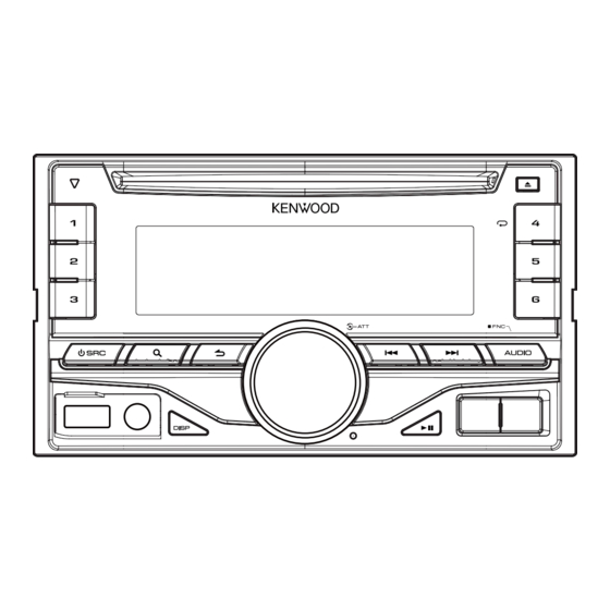
SECTION 4 ADJUSTMENT TEST MODE 4.1.1 Panel SEARCH RETURN DISP ACCENT A symbol " " in the key column indicates that the key should be pressed and hold for 1 second or longer. 4.1.2 How to enter each Test Mode Test Mode name Operation Production Test Mode... -
Page 16: Power Off
Production Test Mode Press and hold [1] key and [3] key and reset. 4.2.1 Default condition when the mode is started It shall be same as normal RST start in other settings than the following. Details Difference in action Period to prohibit TEL/LINE MUTE immediately after activation 1 second (normally 10seconds) CD Mecha Initialize Action... -
Page 17: Display Content
Display content Details Operation Serial No. display (8-digit) Serial No. display *Displays ASCII 2 (Toggle) "********" is displayed if there is no registration All lights ON (Switch with other display) All lights ON Disc Eject number Display Disc Eject number of times. of times display MAX 65535 (times) 3 (Toggle) - Page 18 Display content Details Operation Performs the SOURCE transition. SOURCE Mode release After the SOURCE transition, normal display for transition each mode resumes. When key is pressed, all lights ON/OFF with toggle RETURN When key is pressed, all lights ON/OFF with toggle RETURN When key is pressed, all lights ON/OFF with toggle DISP...
- Page 19 4.2.6 Sirius XM Test Mode Specification Perform a communication test with the Sirius XM Tuner SXV100. If the test result is OK, 1kHz signal is output from the internal tone generator of the SXV100. Without preconditions, in the test mode, start in a state of receiving 0ch. Press the [RETURN] key to switch the signals in the order of L/R →...
- Page 20 4.2.8 BT Test Mode Specification Initial condition of the BT MODE (BT source) will display as following. Status Display content Details BT MODE BT MODE display BT module error display P-CON is off at the time of an error. (Error display appears and P-CON is turned OFF when switched to the BT source) P-CON recovers with Power OFF/ON.
- Page 21 4.2.8.2 Operations during internal loop back Display content Details Operation MIC gain switching Down with [ ] key, Up with [ ] key *1: This is a function to clear the BT memory information recorded in the EEPROM and the FLASH memory to be initialized with the "Data flash clear"...
- Page 22 Service Test Mode In the STANDBY source, while pressing and holding [SEARCH] key, press [AUDIO] key for 7 seconds. (Starting to press [SEARCH] key and [AUDIO] key at the same time can not be entered into the mode) 4.3.1 Default condition when the mode is started It shall be same as normal activation.
- Page 23 4.3.5 CD Error Information Display Mode Display content Details Operation CD Mecha error log DISP Transit to CD error information display mode. display CD Mecha error log Mecha error history 1,2,3 (latest) display #: History No. (1,2,3) xx: kind of errors, "- -" when there is none Displayed in zero suppression when the number of the errors is 1 digit.
- Page 24 Service Information Clear Mode Press and hold [2] key and [5] key and reset. 4.4.1 Default condition when the mode is started It shall be same as normal activation. 4.4.2 Mode structure Service Information Clear Mode can be executed independent of the current source. 4.4.3 Mode content After entering this mode, Syscon shall clear the information stored for service and output the result to the display tube.
- Page 25 DC Error Information Mode Press and hold [3] key and [6] key and reset. 4.5.1 Default condition when the mode is started It shall be same as normal activation. 4.5.2 Mode structure DC Error Information Mode can be executed independent of the current source. 4.5.3 Mode content Syscom shall display the following information after entering this mode.
- Page 26 Version Display Mode In the STANDBY source, while pressing and holding [RETURN] key, press [DISP] key. 4.7.1 Default condition when the mode is started Same as normal start-up. 4.7.2 Mode structure Version display mode can be executed independent of the current source. 4.7.3 Mode content Syscom shall display the following information after entering this mode.
- Page 27 4.10 Security Code Force Delete mode (Only for European models) While pressing and holding [ ] key, press [SEARCH] key for 3 seconds. 4.10.1 Mode transition method Transit to this mode by pressing the above keys, and "- - - -" disappears. 4.10.2 Simplified forced deletion of the security code Clear the security code by the following operations.
- Page 28 4.11.5 Common operation mode Operation Display content Details Signal: 0x00 ~ 0x04(hex) Signal Strength 00 ~ 04 are displayed in "##". Tuner STS:(hex) "##" Bit0: PLL Lock, Bit1: Ant Det Bit2: Ant Undr, Bit3: Ant Ovr Tuner Status Bit4: RF AGC Eng, Bit5: IF AGC Eng Bit6,Bit7: Reserved ENSA Lock Status:(hex) "##"...
- Page 29 Operation Display content Details [Extended channels] Receiver State:(hex) "##" Bit0: TB[otdm], Bit1:S2B[otdm] Receiver State Bit2: S1B[otdm], Bit3: Pipe[LckB] Bit4: TA [otdm], Bit5: S2A[otdm] Bit6: S1A[otdm], Bit7: Pipe[LckA] [Extended channels] OBER Sat 1A OBER S1A: 0 ~ 100 (DEC) "###" [Extended channels] OBER Sat 1B OBER S1B: 0 ~ 100 (DEC) "###"...
-
Page 30: Section 5 Troubleshooting
4.11.6 Clear NVM Mode/ Init Code Press [VOL] knob Press [VOL] knob CLEAR NVM Press [RETURN] key Turn [VOL] knob INIT CODE Press [VOL] knob CLEARING Blinking 500ms Press [RETURN] key SECTION 5 TROUBLESHOOTING This service manual does not describe TROUBLESHOOTING. (No.WA063<Rev.003>)30/31... - Page 31 JVC KENWOOD Corporation Car Electronics Business Group 2967-3, Ishikawa-machi, Hachioji-shi, Tokyo, 192-8525, Japan (No.WA063<Rev.003>) Printed in Japan...
-
Page 32: Schematic Diagrams
SCHEMATIC DIAGRAMS DUAL SIZED CD RECEIVER DPX-U5130 DPX-U5130BT DPX300U DPX305U DPX405BT DPX500BT DPX5130BTPT4 DPXU5130MM3 (No.WA063<Rev.003>)1/16... - Page 33 PRECAUTIONS ON SCHEMATIC DIAGRAMS Due to the improvement in performance, some part numbers shown in the circuit diagrams may not agree with those indicated in the Parts List. The parts numbers, values and rated voltage etc. in the Schematic Diagrams are for reference only.
- Page 34 BLOCK DIAGRAM J131 ELECTRIC UNIT B.U. DC CN B.U. CN891 J461 IC201 J231 CN401 Steering PWIC PRE_OUT REMO REAR MIC FRONT/REAR/SW Q231 Q232 IC461 IC462 Q233 Q234 SW_5V Q235 Q236 LEVEL SHIFT DC_3V3 BU_3V3 MUTE IC251 Q237 IC301 Q132 DC_6V BU_DET BU_DET TUN_1V2...
- Page 35 ELECTRIC UNIT-1 (X34-747x-xx) ?R167 TP461 TP465 *J461 TP467 QNZ0907-001 DC_CN For NET TP462 POWER IC TP464 *R469 TP463 TP468 (BACK SIDE 1/4W of Head Unit) ?R466 *R461 *R462 *R470 IC201 TB2931HQ ?C464 1/4W TU_TX J131 E58-0991-05 For NET 0.01u *R467 TP466 GND_A TU_RX...
- Page 36 0-11 DTA123JUA 1000p QNN0866-001 TDA7720B-X L41-6885-52(9) L41-6885-52(9) L41-4785-52(9) 256k C-1240WE DPX305U 2-72 DTA123JUA 1000p QNN0868-001 TDA7718B-X L41-6885-52(9) L41-6885-52(9) L41-4785-52(9) C-1240WM DPX-U5130 0-22 DTA123JUA 1000p QNN0868-001 TDA7718B-X L41-1095-52(9) L41-3395-52(9) L41-8285-52(9) C-1240WH DPX-U5130 4-11 DTA123JUA 4700p QNN0868-001 TDA7718B-X L41-1095-52(9) L41-3395-52(9) L41-8285-52(9) C-1240WJ...
- Page 37 SWITCH UNIT (X16-7430-1x) *TEL LED LCD BACK LIGHT KEY LED KEY LED TRIANGLE LED (BT MODEL) LCD DISPLAY * Refer to 2.2 LCD DISPLAY INTERNAL SCHEMATIC DIAGRAM B38-1247-05 (Attention) The listed voltages are measured,for instance,by the multimeter with impedance of DC20kohm/V for 0-10 destination. For parts denoted by "...
- Page 38 BLUETOOTH UNIT (X17-2220-10) E41-3376-05 LINEOUT_L LINEOUT_L L77-3873-05 A_GND NOR_XA16 LINEOUT_R LINEOUT_R 3.3k VOUT MIC_IN+ NOR_XA15 MIC_P TP20 VDD1 VSS54 NOR_XA14 NOR_XD15 N.C. 0.1u NOR_XD0 BYTE DQ15 STBY MIC_IN- NOR_XA13 VSS2 VDDQ3 VSSQ52 MIC_N NOR_XA12 NOR_XD14 USB1_D+ NOR_XD15 0.1u NOR_XD1 BU18TD3WG DQ15/A_1 USB_D+ DQ14...
- Page 39 CD PLAYER UNIT (X32-6560-00) TP56 TP55 TP53 TP54 TP47 TP43 FCS- FCS+ TRK+ TRK- E41-3423-05 FCS- FCS- 15 FCS+ FCS+ 14 TRK+ TRK+ 13 TRK- TRK- 12 GND 11 A 10 PICK UP VREF TP51 TP50 TP49 TP48 TP46 TP45 TP52 Vref TP10...
- Page 40 ELECTRIC UNIT X34-747x-xx (J76-0856-02) C138 D201 J461 C223 C224 J231 D202 D463 IC201 D140 R156 C206 D141 D137 IC462 L131 C233 C214 R155 C212 C235 C211 R205 J131 C213 R206 R476 D139 C217 C465 C215 R145 C216 C234 D134 R131 C218 D251 CN401...
- Page 41 ELECTRIC UNIT X34-747x-xx (J76-0856-02) C225 F231 C219 R461 C140 C462 Q232 R237 Q231 C241 C239 R245 R239 R732 Q235 Q233 C238 C237 C242 C240 R234 R233 D360 R246 R240 Q236 Q234 TP150 C380 L380 TP149 C361 C381 C301 C316 R398 R304 TP62 C311...
- Page 42 SWITCH UNIT X16-7430-1x (J76-0857-02) IC602 D616 D611 D602 D615 D617 S613 S601 S605 J602 S618 S608 S617 S602 J601 D605 D606 S606 D608 S603 S614 S610 S607 No.WA063 created date:2013-06-12 (No.WA063<Rev.003>)11/16...
- Page 43 SWITCH UNIT X16-7430-1x (J76-0857-02) C641 R675 R643 R641 R642 R686 R603 REMO IC601 R622 R687 R688 R623 C605 R689 R636 C607 R690 Q613 C685 R624 Q612 SYSDATA C606 Q611 R682 R681 LCDRST Q610 R683 C681 C684 IC604 R635 L602 C686 PANDATA R639 C604...
- Page 44 BLUETOOTH UNIT X17-2220-10 (J76-0854-02) No.WA063 created date:2013-06-12 (No.WA063<Rev.003>)13/16...
- Page 45 BLUETOOTH UNIT X17-2220-10 (J76-0854-02) TP19 TP17 TP18 TP16 TP30 J76-0854-02 X17-2220-10 TP20 TP29 No.WA063 created date:2013-06-12 (No.WA063<Rev.003>)14/16...
- Page 46 CD PLAYER UNIT X32-6560-00 (J76-0842-02) J76-0842-02 X32-6560-00 FCS- FCS+ TRK- TRK+ E IOP+ Vref IOP- DAC3.3V CD-R CD-L CMD-SI SW3.3V CD-RESET CMD-CCE DGND RFRP DGND SSIRX CMD-BUCK DRV-MUTE SW3.3V SW1.5V SSIWS SLED IN/EJECT R103 CD-G SSITX SPINDLE- MGND SPINDLE+ SSISCL SLED OUT/LOAD CD-MUTE No.WA063...
- Page 47 CD PLAYER UNIT X32-6560-00 (J76-0842-02) LIM SW R102 No.WA063 created date:2013-06-12 (No.WA063<Rev.003>)16/16...
-
Page 48: Parts List
PARTS LIST DUAL SIZED CD RECEIVER DPX-U5130 DPX-U5130BT DPX300U DPX305U DPX405BT DPX500BT DPX5130BTPT4 DPXU5130MM3 (No.WA063<Rev.003>)1/17... - Page 49 PRECAUTIONS ON SCHEMATIC DIAGRAMS Due to the improvement in performance, some part numbers shown in the circuit diagrams may not agree with those indicated in the Parts List. The parts numbers, values and rated voltage etc. in the Schematic Diagrams are for reference only.
- Page 50 EXPLODED VIEW (UNIT) Block No.200 *Except *DPX5130BTPT4 DPX5130BTPT4 KDPXU5130MM3 KDPXU5130MM3 DME1 (ELECTRIC) (BLUETOOTH) (SWITCH) Parts with the exploded numbers larger than 700 are not supplied. No.WA063 created date:2013-10-02 (No.WA063<Rev.003>)3/17...
- Page 51 MODEL MARK MODEL MARK MODEL MARK MODEL MARK DPX500BT DPX300U DPX-U5130BT DPX-U5130 DPX5130BTPT4 KDPXU5130MM3 DPX405BT DPX305U DPX-U5130 Safe Symbol No. Parts No. Parts Name Description Local EXPLODED VIEW (UNIT) <200> E30-6939-05 DC CORD K0,K1,M1,M2,M4,H1 E30-6940-15 DC CORD E1,E2 E30-8314-05 DC CORD...
- Page 52 MODEL MARK MODEL MARK MODEL MARK MODEL MARK DPX500BT DPX300U DPX-U5130BT DPX-U5130 DPX5130BTPT4 KDPXU5130MM3 DPX405BT DPX305U DPX-U5130 Safe Symbol No. Parts No. Parts Name Description Local H54-5313-03 ITEM CARTON CASE H54-5314-03 ITEM CARTON CASE M2,H1 H54-5382-03 ITEM CARTON CASE H54-5409-03...
- Page 53 EXPLODED VIEW (CD MECHANISM: X92-6800-00) Block No.130 Grease W01-1738-08 W01-2067-08 FPC1 DPU1 Back view Back view Parts with the exploded numbers larger than 800 are not supplied. No.WA063 created date:2013-06-12 (No.WA063<Rev.003>)6/17...
- Page 54 MODEL MARK MODEL MARK MODEL MARK MODEL MARK DPX500BT DPX300U DPX-U5130BT DPX-U5130 DPX5130BTPT4 KDPXU5130MM3 DPX405BT DPX305U DPX-U5130 Safe Symbol No. Parts No. Parts Name Description Local EXPLODED VIEW (CD MECHANISM: X92-6800-00) <130> X94-2230-00 MD CHASSIS ASSY X94-2240-00 LOADING MOTOR ASSY...
- Page 55 MODEL MARK MODEL MARK MODEL MARK MODEL MARK DPX500BT DPX300U DPX-U5130BT DPX-U5130 DPX5130BTPT4 KDPXU5130MM3 DPX405BT DPX305U DPX-U5130 Safe Symbol No. Parts No. Parts Name Description Local ELECTRIC UNIT (X34-747x-xx) <X34> LV5684PVD IC(ANALOGUE) IC21 XC6217A12BM-G IC(MOS-IC) 1.25V IC51 BD9876EFJ IC(MOS-IC) 3.0A DOWN DCDC,1CH...
- Page 56 MODEL MARK MODEL MARK MODEL MARK MODEL MARK DPX500BT DPX300U DPX-U5130BT DPX-U5130 DPX5130BTPT4 KDPXU5130MM3 DPX405BT DPX305U DPX-U5130 Safe Symbol No. Parts No. Parts Name Description Local CD04AS0J101M ELECTRO 100UF 6.3V M CK73GB1A105K CHIP C 1.0UF 10V K CK73GB1A105K CHIP C 1.0UF 10V K...
- Page 57 MODEL MARK MODEL MARK MODEL MARK MODEL MARK DPX500BT DPX300U DPX-U5130BT DPX-U5130 DPX5130BTPT4 KDPXU5130MM3 DPX405BT DPX305U DPX-U5130 Safe Symbol No. Parts No. Parts Name Description Local C337 CK73GB1H682K CHIP C 6800PF 50V K C338 CK73GB1H682K CHIP C 6800PF 50V K...
- Page 58 MODEL MARK MODEL MARK MODEL MARK MODEL MARK DPX500BT DPX300U DPX-U5130BT DPX-U5130 DPX5130BTPT4 KDPXU5130MM3 DPX405BT DPX305U DPX-U5130 Safe Symbol No. Parts No. Parts Name Description Local R133 RK73GB2A223J CHIP R 22K J 1/10W R134 RK73FB2B154J CHIP R 150K J 1/8W...
- Page 59 MODEL MARK MODEL MARK MODEL MARK MODEL MARK DPX500BT DPX300U DPX-U5130BT DPX-U5130 DPX5130BTPT4 KDPXU5130MM3 DPX405BT DPX305U DPX-U5130 Safe Symbol No. Parts No. Parts Name Description Local R476 RK73GB2A221J CHIP R 220 J 1/10W K0,K1 R477 RK73GB2A221J CHIP R 220 J 1/10W...
- Page 60 MODEL MARK MODEL MARK MODEL MARK MODEL MARK DPX500BT DPX300U DPX-U5130BT DPX-U5130 DPX5130BTPT4 KDPXU5130MM3 DPX405BT DPX305U DPX-U5130 Safe Symbol No. Parts No. Parts Name Description Local L92-0639-05 CHIP FERRITE 100MHZ L92-0612-05 CHIP FERRITE 100MHZ L33-2440-05 SMALL FIXED 33UH INDUCTOR L92-0612-05...
- Page 61 MODEL MARK MODEL MARK MODEL MARK MODEL MARK DPX500BT DPX300U DPX-U5130BT DPX-U5130 DPX5130BTPT4 KDPXU5130MM3 DPX405BT DPX305U DPX-U5130 Safe Symbol No. Parts No. Parts Name Description Local D610 B30-3259-05 K0,K1,M1,M2,M3,E1,E2 D610 NSSM065T-X D611 B30-3259-05 K0,K1,M1,M2,M3,E1,E2 D611 NSSM065T-X D615 B30-3259-05 K0,K1,M1,M2,M3,E1,E2 D615...
- Page 62 MODEL MARK MODEL MARK MODEL MARK MODEL MARK DPX500BT DPX300U DPX-U5130BT DPX-U5130 DPX5130BTPT4 KDPXU5130MM3 DPX405BT DPX305U DPX-U5130 Safe Symbol No. Parts No. Parts Name Description Local S608 NSW0246-001X TACT SWITCH S609 NSW0246-001X TACT SWITCH S610 NSW0246-001X TACT SWITCH S611 NSW0246-001X...
- Page 63 MODEL MARK MODEL MARK MODEL MARK MODEL MARK DPX500BT DPX300U DPX-U5130BT DPX-U5130 DPX5130BTPT4 KDPXU5130MM3 DPX405BT DPX305U DPX-U5130 Safe Symbol No. Parts No. Parts Name Description Local RK73HB1J822J CHIP R 8.2K J 1/16W K0,M1,M3,E1 RK73HB1J471J CHIP R 470 J 1/16W K0,M1,M3,E1...
- Page 64 MODEL MARK MODEL MARK MODEL MARK MODEL MARK DPX500BT DPX300U DPX-U5130BT DPX-U5130 DPX5130BTPT4 KDPXU5130MM3 DPX405BT DPX305U DPX-U5130 Safe Symbol No. Parts No. Parts Name Description Local CK73HB1A104K CHIP C 0.10UF 10V K CK73HB0J105K CHIP C 1.0UF 6.3V K CK73HB1A104K CHIP C 0.10UF 10V K...