Sony CDX-L380X Service Manual
Hide thumbs
Also See for CDX-L380X:
- Operating instructions manual (112 pages) ,
- Installation/connections (2 pages) ,
- Installation/connections manual (11 pages)
Table of Contents
Advertisement
SERVICE MANUAL
Ver 1.1 2003. 06
• The tuner and CD sections have no adjustments.
CD player section
Signal-to-noise ratio
90 dB
Frequency response
10 – 20,000 Hz
Wow and flutter
Below measurable limit
Tuner section
FM
Tuning range
87.5 – 108.0 MHz
Aerial terminal
External aerial connector
Intermediate frequency 10.7 MHz/450 kHz
Usable sensitivity
8 dBf
Selectivity
75 dB at 400 kHz
Signal-to-noise ratio
66 dB (stereo),
72 dB (mono)
Harmonic distortion at 1 kHz
0.6% (stereo),
0.3% (mono)
Separation
35 dB at 1 kHz
Frequency response
30 – 15,000 Hz
MW/LW
Tuning range
MW: 531 – 1,602 kHz
LW: 153 – 279 kHz
Aerial terminal
External aerial connector
Intermediate frequency 10.7 MHz/450 kHz
Sensitivity
MW: 30 µV
LW: 40 µV
Power amplifier section
Outputs
Speaker outputs
(sure seal connectors)
Speaker impedance
4 – 8 ohms
Maximum power output 45 W × 4 (at 4 ohms)
Sony Corporation
9-874-229-02
2003F04-1
e Vehicle Company
© 2003. 06
Published by Sony Engineering Corporation
CDX-L380X
Model Name Using Similar Mechanism
CD Drive Mechanism Type
Optical Pick-up Name
SPECIFICATIONS
General
Outputs
Inputs
Tone controls
Power requirements
Dimensions
Mounting dimension
Mass
Supplied accessories
Design and specifications are subject to change without
notice.
FM/MW/LW COMPACT DISC PLAYER
AEP Model
UK Model
CDX-CA700/CA700X
MG-393XA-121//Q
KSS-720A
Audio outputs
Power aerial relay control
lead
Telephone ATT control lead
Bass ±9 dB at 100 Hz
Treble ±9 dB at 10 kHz
12 V DC car battery
(negative ground)
Approx. 178 × 50 × 177 mm
(w/h/d)
Approx. 182 × 53 × 162 mm
(w/h/d)
Approx. 1.2 kg
Parts for installation and
connections (1 set)
Front panel case (1)
1
Advertisement
Chapters
Table of Contents

Related Manuals for Sony CDX-L380X


Summary of Contents for Sony CDX-L380X
- Page 1 Speaker outputs (sure seal connectors) Speaker impedance 4 – 8 ohms Maximum power output 45 W × 4 (at 4 ohms) FM/MW/LW COMPACT DISC PLAYER Sony Corporation 9-874-229-02 2003F04-1 e Vehicle Company © 2003. 06 Published by Sony Engineering Corporation...
- Page 2 COMPONENTS IDENTIFIED BY MARK 0 OR DOTTED LINE WITH MARK 0 ON THE SCHEMATIC DIAGRAMS AND IN THE PARTS LIST ARE CRITICAL TO SAFE OPERATION. REPLACE THESE COMPONENTS WITH SONY PARTS WHOSE PART NUMBERS APPEAR AS SHOWN IN THIS MANUAL OR IN SUPPLEMENTS PUBLISHED BY SONY.
-
Page 3: Printed Wiring Board -Main Section
CDX-L380X • UNLEADED SOLDER Boards requiring use of unleaded solder are printed with the lead free mark (LF) indicating the solder contains no lead. (Caution: Some printed circuit boards may not come printed with the lead free mark due to their particular size.) : LEAD FREE MARK Unleaded solder has the following characteristics. -
Page 4: Table Of Contents
CDX-L380X TABLE OF CONTENTS 1. GENERAL Location of controls ..............5 Connections ................6 2. DISASSEMBLY 2-1. Sub Panel Assy ..............7 2-2. CD Mechanism Block ............8 2-3. Main Board ................. 8 2-4. Heat Sink ................9 2-5. Chassis (T.U) Assy .............. 9 2-6. -
Page 5: General
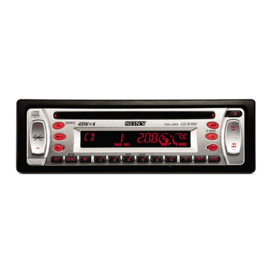
CDX-L380X SECTION 1 GENERAL This section is extracted from instruction manual. Location of controls Refer to the pages listed for details. : During playback : During radio reception RADIO SOURCE D-BASS SEEK MODE SHUF A T T SENS DSPL RELEASE... -
Page 6: Connections
REMOTE IN CDX-L380X/L400X seulement Tulpstekkersnoer (niet bijgeleverd) von Autoantenne Hinweis zum Anschließen der Antenne CDX-L410/L420V seulement Alleen voor de CDX-L380X/L400X AUDIO OUT de l’antenne de la voiture Wenn Ihre Fahrzeugantenne der REAR Alleen voor de CDX-L410/L420V dall’antenna dell’auto ISO-Norm (ISO = International Nota per il collegamento dell’antenna... -
Page 7: Disassembly
CDX-L380X SECTION 2 DISASSEMBLY Note : This set can be disassemble according to the following sequence. 2-5. CHASSIS (T.U) ASSY 2-1. SUB PANEL ASSY (Page 9) (Page 7) 2-6. DISC IN BOARD 2-7. SERVO BOARD 2-2. CD MECHANISM BLOCK (Page 10) -
Page 8: Cd Mechanism Block
CDX-L380X 2-2. CD MECHANISM BLOCK 7 bracket (CD) 5 CD mechanism block 6 PTT 2.6x6 2 PTT 2.6x6 1 PTT 2.6x6 4 CNP301 2-3. MAIN BOARD 4 ground point screw 6 MAIN board (PTT 2.6x6) 5 ground point screws (PTT 2.6x6) 3 PTT 2.6x6... -
Page 9: Heat Sink
CDX-L380X 2-4. HEAT SINK 4 heat sink 3 PTT 2.6x12 2 PTT 2.6x16 1 PTT 2.6x12 2-5. CHASSIS (T.U) ASSY 2 P 2x3 3 P 2x3 1 Unsolder the 4 chassis (T.U) assy lead wires. black white... -
Page 10: Disc In Board
CDX-L380X 2-6. DISC IN BOARD 4 guide (disc) 1 PS 2x3 2 DISC IN board 3 claws 2-7. SERVO BOARD 7 SERVO board 6 PS 2x4 5 PS 2x4 2 Removal the solders. 8 connector 1 CN3 3 P 2x3... -
Page 11: Arm Roller Assy
CDX-L380X 2-8. ARM ROLLER ASSY • When installing, take note of the positions arm (roller) and washers. (Fig. 1) 3 retaing ring (roller) bearing (roller) bearing (roller) 4 bearing (roller) washer (RA) retaing ring (roller) washer (RA) Fig. 1 5 shaft roller assy... -
Page 12: Optical Pick-Up Block
CDX-L380X 2-10. OPTICAL PICK-UP BLOCK 4 P 2x3 1 P 2x3 5 leaf spring (feed) 2 sled motor assy 3 optical pick-up block 6 shaft (feed) assy... -
Page 13: Diagrams
Not used. (Open) TELATT Telephone attenuate detection input NC (VCC) — Not used. (Connect to VDD in this set) UNISO SONY BUS data output UNISI SONY BUS data input UNICKO SONY BUS clock output Not used. (Open) I2C_SIO C BUS serial data input/output —... - Page 14 CDX-L380X Pin No. Pin Name Pin Description RFOK CD RFOK signal input CD_RST CD reset signal output CD command/parameter signal output CD strobe signal output X_EN CD crystal oscillator control output LIMIT CD limit switch input Not used. (Fixed at H in this set)
-
Page 15: Block Diagram -Cd Section
CDX-L380X 3-2. BLOCK DIAGRAM — CD SECTION — RF AMP,DIGITAL SERVO, DIGITAL SIGNAL PROCESSOR OPTICAL PICK-UP (KSS-720A) (Page 16) TUNER SECTION LOUT SYSTEM CONTROL ROUT IC501 (1/3) CONV R-CH DEMOD PACK CD PACK DSUB CODE TSTB PROCESS TSTB CONV. CD TSO... -
Page 16: Block Diagram -Tuner Section
CDX-L380X 3-3. BLOCK DIAGRAM — TUNER SECTION — POWER AMP ELECTRONIC VOLUME IC404 IC401 CNP601 (Page 15) OUT FL SECTION TUNER UNIT TU10 SE L ANTFM OUT RL (ANTENNA) Q451 Q431 ANTAM AM DET 16 AUX MUTE MUTE 4 STBY... -
Page 17: Block Diagram -Display Section
CDX-L380X 3-5. CIRCUIT BOARDS LOCATION 3-4. BLOCK DIAGRAM — DISPLAY SECTION — SUB (CD) board DISC IN board SYSTEM CONTROL LCD DRIVE IC501 (3/3) IC901 KEY IN0 LCD SO KEY MATRIX LCD901 LIMIT board LSW900-922 LCD CKO KEY IN1 LCD CE... -
Page 18: Printed Wiring Boards -Cd Mechanism Section
CDX-L380X 3-6. PRINTED WIRING BOARDS — CD MECHANISM SECTION — • Refer to page 17 for Circuit Boards Location. : Uses unleaded solder. THIS NOTE IS COMMON FOR PRINTED WIRING BOARDS AND SCHEMATIC DIAGRAMS. (In addition to this, the necessary note is printed in each block.) - Page 19 CDX-L380X : Uses unleaded solder. TP77 TP78 TP62 TP82 TP48 TP66 TP80 TP84 (Page 21) TP83 TP60 TP12 TP11 TP50 TP47 C9 C10 TP64 TP10 TP51 TP59 TP89 TP52 TP71 TP56 TP22 TP58 TP72 TP24 TP23 TP25 TP61 TP76 TP88...
-
Page 20: Schematic Diagram -Cd Mechanism Section
CDX-L380X • Refer to page 17 for Waveforms and page 18 for Common Note on Schematic Diagram. 3-7. SCHEMATIC DIAGRAM — CD MECHANISM SECTION — • Refer to page 26 for IC Block Diagrams. TP9 TP8 TP77 TP78 TP89 TP79... -
Page 21: Printed Wiring Board -Main Section
CDX-L380X 3-8. PRINTED WIRING BOARD — MAIN SECTION — • Refer to page 17 for Circuit Boards Location and page 18 for Common Note on Printed Wiring Boards. : Uses unleaded solder. J401 JW127 IC404 JW126 F901 C434 C806 C475... -
Page 22: Schematic Diagram -Main Section (1/2)
CDX-L380X • Refer to page 17 for Waveforms and page 18 for Common Note on Schematic Diagram. 3-9. SCHEMATIC DIAGRAM — MAIN SECTION (1/2) — • Refer to page 26 for IC Block Diagrams. C802 IC20 R27 C27 C406 C405... -
Page 23: Schematic Diagram -Main Section (2/2)
CDX-L380X 3-10. SCHEMATIC DIAGRAM — MAIN SECTION (2/2) — • Refer to page 18 for Common Note on Schematic Diagram and page 26 for IC Block Diagrams. C455 C477 IC404 J401 C431 R431 C433 R433 D471 D472 Q431 R432 C465... -
Page 24: Printed Wiring Board -Key Section
CDX-L380X 3-11. PRINTED WIRING BOARD — KEY SECTION — • Refer to page 17 for Circuit Boards Location and page 18 for Common Note on Printed Wiring Boards. : Uses unleaded solder. LSW900 LED921 LED922 LSW902 LSW912 LSW903 LSW911 LCD901... -
Page 25: Schematic Diagram -Key Section
CDX-L380X 3-12. SCHEMATIC DIAGRAM — KEY SECTION — • Refer to page 18 for Common Note on Schematic Diagram. LSW903 LSW902 LSW914 LSW921 LSW907 LSW913 CN901 LED921 LSW904 LSW901 LSW915 LSW920 LSW908 LSW912 D991 R993 R996 PL901 R997 R998 R994... -
Page 26: Ic Block Diagrams
CDX-L380X 3-13. IC BLOCK DIAGRAMS IC1 µPD63711GC-8EU IC2 BA5810FP-E2 71 70 BIAS LOADING PRE MICROCOMPUTER INTERFACE OPIN4+ FWD REV AGCI 50 C2D3 – OPIN4– COMPARATOR 49 C2D2 LDCONT CD-TEXT DECODER 48 C2D1 POWER OPOUT4 SUB-CODE PROCESSOR SAVE 47 C1D2 MEMORY... - Page 27 CDX-L380X IC401 TDA7402TR 32 31 30 29 28 27 26 25 24 23 MONO SUPPLY FADER MIXER SUBWOOFER MONO MONO +PHASE FADER FADER CONTROL ACINLF OUTPUT CONTROL SWINR SWINL MUTE AC OUTR VOICE AC OUTL BANDPASS C-BUS QUAL. QUAL BASS...
-
Page 28: Exploded Views
CDX-L380X SECTION 4 EXPLODED VIEWS NOTE: • The mechanical parts with no reference • Color Indication of Appearance Parts The components identified by number in the exploded views are not supplied. mark 0 or dotted line with mark. Example : •... -
Page 29: Front Panel Section
CDX-L380X 4-2. FRONT PANEL SECTION not supplied (KEY board) LCD901 not supplied Ref. No. Part No. Description Remark Ref. No. Part No. Description Remark A-3315-955-A PANEL COMPLETE ASSY, FRONT 3-235-382-01 PLATE (LCD), GROUND 3-224-869-03 BUTTON (RELEASE/U) 1-694-781-11 CONDUCTIVE BOARD, CONNECTION... -
Page 30: Cd Mechanism Section (1)
CDX-L380X 4-3. CD MECHANISM SECTION (1) (MG-393XA-121//Q) not supplied supplied not supplied not supplied not supplied M903 Ref. No. Part No. Description Remark Ref. No. Part No. Description Remark A-3315-247-B CHASSIS (T.U) ASSY 3-225-784-01 SPRING (RA3), TENSION 3-931-909-01 SPRING (LR), TENSION... -
Page 31: Cd Mechanism Section (2)
CDX-L380X 4-4. CD MECHANISM SECTION (2) (MG-393XA-121//Q) not supplied Ref. No. Part No. Description Remark Ref. No. Part No. Description Remark X-3378-956-8 ARM ASSY, CHUCKING A-3315-243-D CHASSIS (M) ASSY 3-931-897-61 DAMPER (T) 3-220-180-01 SPRING (TR2), TENSION 3-039-627-01 LEVER (D) 3-931-881-03 LEVER (LOCK) -
Page 32: Cd Mechanism Section (3)
CDX-L380X 4-5. CD MECHANISM SECTION (3) (MG-393XA-121//Q) M901 M902 The components identified by mark 0 or dotted line with mark. 0 are critical for safety. Replace only with part number specified. Ref. No. Part No. Description Remark Ref. No. Part No. -
Page 33: Electrical Parts List
CDX-L380X SECTION 5 DISC IN ELECTRICAL PARTS LIST NOTE: • Due to standardization, replacements in • Items marked “*” are not stocked since The components identified by mark 0 or dotted line with mark. the parts list may be different from the they are seldom required for routine service. - Page 34 CDX-L380X LIMIT MAIN Ref. No. Part No. Description Remark Ref. No. Part No. Description Remark R916 1-216-825-11 METAL CHIP 2.2K 1/10W A-3274-611-A MAIN BOARD, COMPLETE R917 1-216-827-11 METAL CHIP 3.3K 1/10W ********************* R918 1-216-829-11 METAL CHIP 4.7K 1/10W R919 1-218-867-11 METAL CHIP 6.8K...
- Page 35 CDX-L380X MAIN Ref. No. Part No. Description Remark Ref. No. Part No. Description Remark C405 1-124-233-11 ELECT 10uF CNP601 1-774-701-11 PIN, CONNECTOR 16P C406 1-162-970-11 CERAMIC CHIP 0.01uF C407 1-162-915-11 CERAMIC CHIP 10PF 0.5PF < DIODE > C411 1-124-233-11 ELECT...
- Page 36 CDX-L380X MAIN Ref. No. Part No. Description Remark Ref. No. Part No. Description Remark JC601 1-216-296-11 SHORT CHIP R433 1-216-833-11 METAL CHIP 1/10W JC602 1-216-296-11 SHORT CHIP R434 1-216-809-11 METAL CHIP 1/10W JC801 1-216-296-11 SHORT CHIP R441 1-216-809-11 METAL CHIP...
- Page 37 CDX-L380X MAIN SERVO Ref. No. Part No. Description Remark Ref. No. Part No. Description Remark R651 1-216-821-11 METAL CHIP 1/10W 1-126-391-11 ELECT CHIP 47uF 6.3V R652 1-216-841-11 METAL CHIP 1/10W 1-162-970-11 CERAMIC CHIP 0.01uF R653 1-216-833-11 METAL CHIP 1/10W 1-162-970-11 CERAMIC CHIP 0.01uF...
- Page 38 CDX-L380X SUB (CD) Ref. No. Part No. Description Remark 1-659-834-21 SUB (CD) BOARD ************** 1-683-665-11 MOTOR FLEXIBLE BOARD ************************************************************* MISCELLANEOUS *************** 1-776-527-61 CORD (WITH CONNECTOR) (ISO) (POWER) X-3378-598-3 CHASSIS (OP) ASSY (including M901) 0 210 8-820-103-11 OPTICAL PICK-UP KSS-720A/K1NP F901...
- Page 39 CDX-L380X AEP Model UK Model SERVICE MANUAL Ver 1.1 2003. 06 SUPPLEMENT-1 File this supplement with the service manual. Subject : Change of Main Board (ENG-03006) When performing service and inspection, check the suffix of the part number of the main board.
- Page 40 CDX-L380X TABLE OF CONTENTS THIS NOTE IS COMMON FOR PRINTED WIRING BOARDS AND SCHEMATIC DIAGRAMS. (In addition to this, the necessary note is 1. Printed Wiring Board –Main Section– ........3 printed in each block.) 2. Schematic Diagram –Main Section (1/2)– ......4 3.
- Page 41 CDX-L380X 1. PRINTED WIRING BOARD — MAIN SECTION — • Refer to page 2 for Common Note on Printed Wiring Boards. J401 JW127 CNP601 JW126 F901 IC404 C434 C806 C475 C444 C464 JC473 C455 C465 JW23 R442 R452 R462 JC601...
-
Page 42: Schematic Diagram -Main Section (1/2)
CDX-L380X 2. SCHEMATIC DIAGRAM — MAIN SECTION (1/2) — • Refer to page 2 for Waveforms and Common Note on Schematic Diagram. C802 IC20 C405 C406 C407 C806 IC B/D C411 JC801 C412 R434 R454 R444 IC401 R464 TU10 C402... -
Page 43: Schematic Diagram -Main Section (2/2)
CDX-L380X 3. SCHEMATIC DIAGRAM — MAIN SECTION (2/2) — • Refer to page 2 for Common Note on Schematic Diagram. C455 C477 IC404 J401 C431 R431 C433 R433 D471 D472 Q431 R432 C465 R452 Q451 C451 D473 CNP601 R451 C453... - Page 44 CDX-L380X MAIN 4. ELECTRICAL PARTS LIST NOTE: Ref. No. Part No. Description Remark Ref. No. Part No. Description Remark • Due to standardization, replacements in • Items marked “*” are not stocked since The components identified by C601 1-135-473-21 ELECT...
- Page 45 CDX-L380X MAIN Ref. No. Part No. Description Remark Ref. No. Part No. Description Remark 1-216-845-11 METAL CHIP 100K 1/10W R528 1-216-845-11 METAL CHIP 100K 1/10W 1-216-841-11 METAL CHIP 1/10W R529 1-216-833-11 METAL CHIP 1/10W 1-216-853-11 METAL CHIP 470K 1/10W R530...
- Page 46 CDX-L380X REVISION HISTORY Clicking the version allows you to jump to the revised page. Also, clicking the version at the upper on the revised page allows you to jump to the next revised page. Ver. Date Description of Revision 2002. 11 2003.