Table of Contents
Advertisement
SERVICE MANUAL
Ver 1.2 2004.05
With CORRECTION-1R
(9-929-025-92)
HCD-ED2 is the tuner, deck, CD and
amplifier section in CMT-ED2.
This systems is equipped with the Dolby* B-type noise
reduction system.
*Dolby noise reduction manufactured under license
from Dolby Laboratories Licensing Corporation.
"DOLBY" and the double-D symbol a are
trademarks of Dolby Laboratories Licensing
Corporation.
Amplifier section
For the U.S. model
AUDIO POWER SPECIFICATIONS
POWER OUTPUT AND TOTAL HARMONIC
DISTORTION:
With 8-ohm loads both channels driven from
90 - 15,000 Hz; rated 15 watts per channel
minimum RMS power with no more than 09.%
total harmonic distortion from 250 milliwatts to
rated output.
North American model:
Continuous RMS power output (reference):
17 + 17 W
(8 ohms at 1 kHz, 10%THD)
European model:
DIN power output (rated):
15 + 15 W
(8 ohms at 1 kHz, DIN)
Continuous RMS power output (reference):
17 + 17 W
(8 ohms at 1 kHz, 10% THD)
Music power output (reference):
35 + 35 W
Other models:
The following measured at 230 V AC, 60 Hz
DIN power output (rated):
15 + 15 W
(8 ohms at 1 kHz, DIN)
Sony Corporation
9-929-025-13
Home Audio Company
2004E02-1
Published by Sony Engineering Corporation
© 2004.05
Model Name Using Similar Mechanism NEW
Mechanism Type
CD
SECTION
Base Unit Type
Optical Pick-up Type
Model Name Using Similar Mechanism NEW
TAPE DECK
SECTION
Tape Transport Mechanism Type
SPECIFICATIONS
Continuous RMS power output (reference):
17 + 17 W
(8 ohms at 1 kHz, 10%THD)
Inputs
MD IN (phono jacks) :
Sensitivity 1,000 mV, impedance
47 kilohm
CD DIGITAL OUT OPTICAL:
optical
PHONES (stereo phone jack):
Accepts headphones with an
impedance of 8 ohms or more
SPEAKER:
Accepts Impedance of 8 to 16
ohms
COMPACT DISC DECK RECEIVER
HCD-ED2
Canadian Model
Australian Model
CDM-61
KSM-331AAN/K1NP
KSS-331A (RP)
CMAL1Z025A
CD player section
System
audio
Laser
Laser output
objective
the Optical
with 7 mm
Wavelength
Frequency response
Tape player section
Recording system 4-track 2-channel stereo
Frequency response (DOLBY NR OFF)
— Continued on next page —
US Model
AEP Model
UK Model
E Model
Compact disc and digital
system
Semiconductor laser
(λ = 780 nm)
Emission duration: continuous
MAX 44.6 µW*
*This output is the value
measured at a distance of
200 mm from the
lens surface on
Pick-up Block
aperture.
780 - 790 nm
2 Hz - 20 kHz (±0.5 dB)
50 - 13,000 Hz (±3 dB),
using a Sony TYPE I cassette
50 - 14,000 Hz (±3 dB),
using a Sony TYPE II cassette
1
Advertisement
Table of Contents

Related Manuals for Sony HCD-ED2


Summary of Contents for Sony HCD-ED2
- Page 1 With CORRECTION-1R UK Model (9-929-025-92) E Model Australian Model HCD-ED2 is the tuner, deck, CD and amplifier section in CMT-ED2. This systems is equipped with the Dolby* B-type noise Model Name Using Similar Mechanism NEW reduction system. *Dolby noise reduction manufactured under license...
- Page 2 LES COMPOSANTS IDENTIFIÉS PAR UNE MARQUE ! SUR LES DIAGRAMMES SCHÉMATIQUES ET LA LISTE DES PIÈCES SONT CRITIQUES POUR LA SÉCURITÉ DE FONCTIONNEMENT. NE REMPLACER CES COMPOSANTS QUE PAR DES PIÈCES SONY DONT LES NUMÉROS SONT DONNÉS DANS CE MANUEL OU DANS LES SUPPLÉMENTS PUBLIÉS PAR SONY.
-
Page 3: Table Of Contents
SAFETY CHECK-OUT TABLE OF CONTENTS After correcting the original service problem, perform the follow- 1. SERVICING NOTE ............4 ing safety checks before releasing the set to the customer: Check the antenna terminals, metal trim, “metallized” knobs, screws, 2. GENERAL ................ -
Page 4: Servicing Note
SECTION 1 SERVICING NOTE Connectiong the extension cable (CMT-ED2) Tape preamp board Relay board Extension cable (23pin)(25cmm) M703-2 W703-1 M703-1 W703-2 Relay board Extension cable (23pin)(25cmm) (CMT-ED2, J-2501-179-A) CD LID Tape preamp board The CD lid of this unit is opened and closed electrically. Opening or closing the CD lid with force when the power plug is not connected to the outlet or the power is OFF may damage the hinge. -
Page 5: General
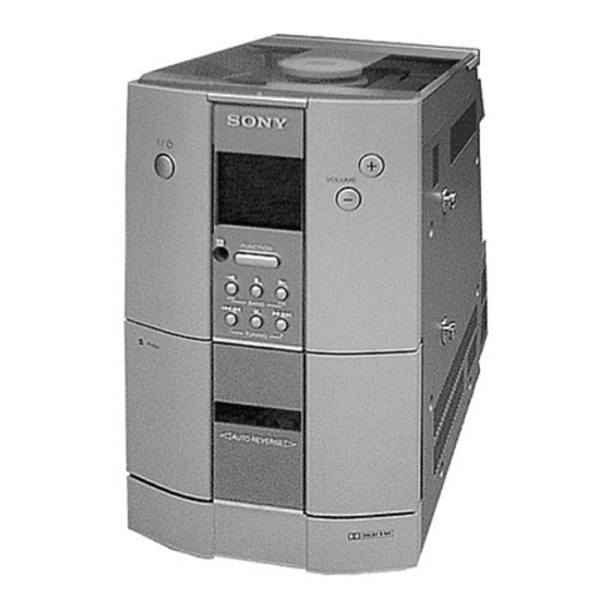
SECTION 2 GENERAL Front Panel LOCATION OF PARTS AND CONTROLS 1 1/u (Power) switch 2 Display window 3 VOLUME + button 4 VOLUME - button 5 FUNCTION 6 ( button 7 p (stop) button 8 ) + + button 9 P button 10 DECK Lid 11 6 Push 12 = 0 - button... -
Page 7: Disassembly
SECTION 3 DISASSEMBLY Note: Follow the disassembly procedure in the numerical order given. 3-1. CD BASE AND BASE UNIT Rotate gear in the direction of arrow. Open the cd door. Three screws (K3x8) Two raber caps !™ Two screws Two hook (BTP3x10) !¡... -
Page 8: Bottom Cover And Front Panel Block
3-3. BOTTOM COVER AND FRONT PANEL Connector (8P) Connector (14P) Bottom cover Front panel block Two screws (BTP3x8) Two claws Screw Solder lug Two screws (BTP3x8) (B2.6x4) 3-4. DOOR COVER AND MECHANICAL (CASSETTE) Two screws (BTP3x8) Two screws Door spring (BTP3x8) Mechanical deck (cassette) -
Page 9: Mechanical Adjustments
SECTION 4 SECTION 5 MECHANICAL ADJUSTMENTS ELECTRICAL ADJUSTMENTS PRECAUTION DECK SECTION 0 dB=0.775V 1. Clean the following parts with a denatured alcohol-moistened 1. Demagnetize the record/playback head with a head damagnetizer. swab : (Do not bring the head demagnetizer close to the erase head.) record/playback heads pinch rollers 2. - Page 10 2. Turn the adjustment screw and check output peaks. If the peaks Tape Speed Adjustment do not match for L-CH and R-CH, turn the adjustment screw so that outputs match within 1 dB of peak. Procedure : Mode : Playback test tape WS-48B frequency counter...
- Page 11 Record Bias Adjustment 2. Mode: Playback Procedure : recorded level meter 1. Mode : Record position MD IN (JK301) 1) 315Hz 50 mV (–23.8 dB) 2) 10kHz AF OSC blank tape 600 Ω CS-123 MD OUT (JK301) attenuator Confirm playback the signal recorded in step 1 become adjustment level as follows.
- Page 12 Note: Clear RF signal waveform means that the shape “◊” can be CD SECTION clearly distinguished at the center of the waveform. Note: RF signal waveform 1. CD Block is basically constructed to operate without adjustment. VOLT/DIV : 200mV TIME/DIV : 500ns Therefore, check each item in order given.
-
Page 13: Diagrams
HCD-ED2 SECTION 6 DIAGRAMS 6-1. CIRCUIT BOARDS LOCATION WAVEFORMS THIS NOTE IS COMMON FOR PRINTED WIRING – BD (CD) SECTION – BOARDS AND SCHEMATIC DIAGRAMS. (In addition to this, the necessary note is printed in each block.) 3.1Vp-p For schematic diagrams. -
Page 14: Schematic Diagram - Bd Section
HCD-ED2 6-2. SCHEMATIC DIAGRAM – BD SECTION – • See page 13 for Waveforms. • See page 15 for Printed Wiring Board. • See page 28 for IC Block Diagrams. • See page 30 for IC Pin Functions. 331A (RP) -
Page 15: Printed Wiring Board - Bd Section
HCD-ED2 6-3. PRINTED WIRING BOARD – BD SECTION – • See page 13 for Circuit Boards Location. S101 S102 S101 SPINDLE SLED LIMITSW MOTOR MOTOR BD BOARD (SIDE B) BD BOARD (SIDE A) CNU103 CNU105 C159 (VC) R159 R158 CNU104... -
Page 16: Schematic Diagram - Function Section
HCD-ED2 6-4. SCHEMATIC DIAGRAM – FUNCTION SECTION – • See page 13 for Waveforms. • See page 17 for Printed Wiring Board. • See page 28 for IC Block Diagrams. • See page 30 for IC Pin Functions. -
Page 17: Printed Wiring Board - Function Section
HCD-ED2 6-5. PRINTED WIRING BOARD – FUNCTION SECTION – • Semiconductor Location • See page 13 for Circuit Boards Location. Ref. No. Location D301 D302 D303 IC301 IC302 IC305 Q301 Q302 Q303 Q304 Q305 Q306 FUNCTION BOARD R325 RELAY L301... -
Page 18: Schematic Diagram - Tape Preamp Section
HCD-ED2 6-6. SCHEMATIC DIAGRAM – TAPE PREAMP SECTION – • See page 13 for Waveforms. • See page 19 for Printed Wiring Board. • See page 28 for IC Block Diagrams. • See page 30 for IC Pin Functions. -
Page 19: Printed Wiring Board - Tape Preamp Section
HCD-ED2 6-7. PRINTED WIRING BOARD – TAPE PREAMP SECTION – • See page 13 for Circuit Boards Location. DOOR MOTOR TAPE PREAMP BOARD CD SW BOARD W193 M193 J180 R191 W193 D191 C191 RELAY BOARD W7031 M194 REC BIAS PB LEVEL... -
Page 20: Schematic Diagram - Display Section
HCD-ED2 6-8. SCHEMATIC DIAGRAM – DISPLAY SECTION – • See page 13 for Waveforms. • See page 21 for Printed Wiring Board. • See page 28 for IC Block Diagrams. • See page 30 for IC Pin Functions. -
Page 21: Printed Wiring Board - Display Section
HCD-ED2 6-9. PRINTED WIRING BOARD – DISPLAY SECTION – • See page 13 for Circuit Boards Location. RELAY BOARD W202 (Page 23) DISPLAY BOARD (SIDE A) DISPLAY BOARD ( SIDE B ) VOL+ R240 R255 D203 M202 S201 D210 R290... -
Page 22: Schematic Diagram - Relay Section
HCD-ED2 Ver 1.2 6-10. SCHEMATIC DIAGRAM – RELAY SECTION – • See page 13 for Waveforms. • See page 23 for Printed Wiring Board. • See page 28 for IC Block Diagrams. • See page 30 for IC Pin Functions. -
Page 23: Printed Wiring Board - Relay Section
HCD-ED2 • Semiconductor 6-11. PRINTED WIRING BOARD – RELAY SECTION – Location • See page 13 for Circuit Boards Location. Ref. No. Location D200 (Page 21) (Page 25) D206 RELAY BOARD ( SIDE B ) D207 POWER AMP DISPLAY D213... -
Page 24: Schematic Diagram - Power Section
HCD-ED2 Ver 1.1 2002.05 6-12. SCHEMATIC DIAGRAM – POWER SECTION – • See page 13 for Waveforms. • See page 25 for Printed Wiring Board. • See page 28 for IC Block Diagrams. • See page 30 for IC Pin Functions. -
Page 25: Printed Wiring Board - Power Section
HCD-ED2 6-13. PRINTED WIRING BOARD – POWER SECTION – Ver 1.1 2002.05 • See page 13 for Circuit Boards Location. POWER IC BOARD ( SIDE A ) • Semiconductor Location Ref. No. Location W504 POWER AMP BOARD SPEAKER D502 D503... -
Page 26: Schematic Diagram - Rds Section
HCD-ED2 6-14. SCEMATIC DIAGRAM – RDS SECTION – • See page 13 for Waveforms. • See page 27 for Printed Wiring Board. • See page 28 for IC Block Diagrams. • See page 30 for IC Pin Functions. -
Page 27: Printed Wiring Board - Rds Section
HCD-ED2 6-15. PRINTED WIRING BOARD – RDS SECTION – • See page 13 for Circuit Boards Location. RDS BOARD L403 L404 X451 TUNER L402 PACK SUPPLIED AS THE M401 ASSEMBLED BLOCK LC451 C452 C404 C453 M451 L405 EXCEPT US, CND... -
Page 28: Ic Block Diagrams
HCD-ED2 Ver 1.2 6-16. IC BLOCK DIAGRAMS • BD Board • FUNCTION Board IC301 M62442 IC101 CXD2587Q ERROR DIGITAL ASYMMETRY DIGITAL CORRECTOR CORRECTION VOLIN1 VOLIN2 LRCK OPERATIONAL AMPLIFIER FOUT1 PCMD FOUT2 INTERFACE DEMODULATOR ANALOG SWITCH F6F1 F6F2 CONVERTER EMPH F5F1... - Page 29 • RDS Board IC451 BU1922 TEST LOGIC AND OUTPUT SELECTOR SWITCH 57kHz ANTI- OSCILLATOR QUALITY BIT RECONSTRUCTION BANDPASS ALIASING GENERATOR FILTER (8th ORDER) FILTER DIVIDER BIPHASE CONTAS LOOP DEFFERENTIAL CLOCKED SYMBOL VARIABLE AND DECODER COMPARATOR DECODER FIXED DIVIDER CLOCK REGENERATION AND SYNC REFERENCE VOLTAGE...
-
Page 30: Ic Pin Functions
6-17. IC PIN FUNCTIONS • IC201 MASTER CONTROL (TC9901) (DYSPLAY Board) Pin Name Function Pin No. XOUT 8MHz Oscillator 8MHz Oscillator RESET CPU reset input TUNED Station detector input STEREO Stereo signal input TEST No Use, Tied to low POWDEC Power down detect REMOTE Remote signal input... - Page 31 Pin Name Function Pin No. FRECSW Tape forward/reverse record sw input 1.7V (2k4) = frecsw on & rrecsw on RRECSW 2.25V (3k9) = frecsw on & rrecsw off 2.89V (6k8) = frecsw off & rrecsw on 5V = frecsw off & rrecsw off PLAYSW Tape play/tape in sw input 1.7V (2k4) = play sw on &...
- Page 32 Pin Name Function Pin No. SEG9 SEG8 SEG7 SEG6 SEG5 LCD segment output SEG4 SEG3 SEG2 SEG1 SEG0 COM3 LCD common 3 output COM2 LCD common 2 output COM1 LCD common 1 output COM0 LCD common 0 output LCD drive power supply –...
-
Page 33: Exploded Views
SECTION 7 EXPLODED VIEWS NOTE: The components identified by • Hardware (# mark) list and accessories and pack- • -XX, -X mean standardized parts, so they may have mark ! or dotted line with mark ing materials are given in the last of this parts list. some difference from the original one. -
Page 34: Rear Panel Section
Ver 1.1 2002.05 7-2. REAR PANEL SECTION (AUS) (EXCEPT US,CND,UK,AUS) (UK) (HK) not supplied (US,CND) not supplied S501 not supplied T501 not supplied not supplied FRONT PANEL Les composants identifiés par The components identified by une marque ! sont critiques pour mark ! or dotted line with mark ! are critical for safety. -
Page 35: Front Panel Section
7-3. FRONT PANEL SECTION Z201 DECK, MECHANICAL Ref. No. Part No. Description Remark Ref. No. Part No. Description Remark 4-225-779-01 PUSH BUTTON 4-225-783-01 GEAR HOLDER 4-225-771-01 SPRING (DOOR), TORSION 4-225-851-01 LCD HOLDER X-4952-472-1 CASS DOOR SUB ASSY 4-225-853-01 LIGHT BAR 1-791-958-11 WIRE (FLAT TYPE) (15 CORE) * 105 A-4428-104-A DISPLAY BOARD, COMPLETE... -
Page 36: Mechanism Deck Section (Cassette)
7-4. MECHANISM DECK SECTION (CASSETTE) not supplied M901 not supplied not supplied not supplied not supplied not supplied supplied not supplied not supplied not supplied supplied supplied not supplied not supplied supplied not supplied not supplied not supplied (including Ref. No. Part No. -
Page 37: Base Unit Section
Ver 1.1 2002.05 7-5. BASE UNIT SECTION (CDM-61) M101 S101 M102 Les composants identifiés par The components identified by mark ! or dotted line with mark une marque ! sont critiques pour ! are critical for safety. la sécurité. Replace only with part number Ne les remplacer que par une specified. -
Page 38: Electrical Parts List
SECTION 8 AC IN ELECTRICAL PARTS LIST Note: • Due to standardization, replacements in the parts list • SEMICONDUCTORS The components identified by In each case, u: µ , for example: may be different from the parts specified in the mark ! or dotted line with mark uA...: µ... - Page 39 CD SW DISPLAY Ref. No. Part No. Description Remark Ref. No. Part No. Description Remark < RESISTOR > A-4428-104-A DISPLAY BOARD, COMPLETE ************************ R101 1-216-077-91 RES,CHIP 1/10W (AEP,UK,MY,SP,KR,TW) R102 1-216-097-91 RES,CHIP 100K 1/10W R103 1-216-077-91 RES,CHIP 1/10W A-4428-244-A DISPLAY BOARD, COMPLETE (US,CND) R104 1-216-085-00 METAL CHIP 1/10W...
-
Page 40: Display Function
DISPLAY FUNCTION Ref. No. Part No. Description Remark Ref. No. Part No. Description Remark < TRANSISTOR > R284 1-247-807-31 CARBON 1/4W Q201 8-729-230-49 TRANSISTOR 2SC2712G-TE85L R285 1-247-807-31 CARBON 1/4W Q216 8-729-230-49 TRANSISTOR 2SC2712G-TE85L R286 1-216-025-91 RES,CHIP 1/10W R287 1-216-025-91 RES,CHIP 1/10W <... - Page 41 FUNCTION Ref. No. Part No. Description Remark Ref. No. Part No. Description Remark C331 1-163-006-11 CERAMIC CHIP 560PF < IC > C332 1-130-495-00 MYLAR 0.1uF C333 1-126-059-11 ELECT 10uF IC301 8-759-495-85 IC M62442FP-A C334 1-130-487-00 MYLAR 0.022uF IC302 8-759-711-85 IC NJM4580E-D-TE2 C335 1-130-488-00 MYLAR 0.027uF...
- Page 42 FUNCTION POWER AMP Ref. No. Part No. Description Remark Ref. No. Part No. Description Remark R341 1-249-437-11 CARBON 1/4W 7-685-872-09 SCREW +BVTT 3X8 (S) R342 1-216-089-91 RES,CHIP 1/10W 1-533-293-11 FUSE HOLDER R344 1-249-421-11 CARBON 2.2K 1/4W F R345 1-249-437-11 CARBON 1/4W <...
- Page 43 POWER AMP Ref. No. Part No. Description Remark Ref. No. Part No. Description Remark C531 1-162-851-11 CERAMIC 0.1uF < IC > C532 1-130-495-00 MYLAR 0.1uF IC501 8-759-701-57 IC NJM78M06FA C538 1-163-035-00 CERAMIC CHIP 0.047uF IC505 8-759-288-53 IC LA5617 C539 1-163-035-00 CERAMIC CHIP 0.047uF C540 1-101-004-00 CERAMIC...
- Page 44 POWER AMP POWER IC Ref. No. Part No. Description Remark Ref. No. Part No. Description Remark 1-249-386-11 CARBON 1/6W F C421 1-124-589-11 ELECT 47uF (AEP,UK,MY,SP,HK,KR,TW,AUS) C423 1-126-157-11 ELECT 10uF R30A 1-216-298-00 METAL CHIP 1/10W C451 1-124-257-00 ELECT 2.2uF (AEP,UK,MY,SP,HK,KR,TW,AUS) R30B 1-216-298-00 METAL CHIP 1/10W C452...
- Page 45 RELAY Ref. No. Part No. Description Remark Ref. No. Part No. Description Remark < VIBRATOR > < IC > X451 1-579-900-21 VIBRATOR, CRYSTAL (4.332MHz) IC650 8-759-925-80 IC SN74HC14ANS-E05 (AEP,UK,MY,SP,HK,KR,TW,AUS) IC651 8-759-925-90 IC SN74HC74ANS-E05 < COIL > ************************************************************** A-4428-106-A RELAY BOARD, COMPLETE L202 1-410-517-11 INDUCTOR 47uH...
- Page 46 TAPE PREAMP Ref. No. Part No. Description Remark Ref. No. Part No. Description Remark A-4428-109-A TAPE PREAMP BOARD, COMPLETE C799 1-101-001-00 CERAMIC 0.001uF C801 1-126-157-11 ELECT 10uF **************************** C802 1-161-772-11 CERAMIC 0.1uF 1-784-361-11 JACK (SMALL TYPE) (PHONES) C799A 1-101-004-00 CERAMIC 0.01uF <...
- Page 47 Ver 1.1 2002.05 TAPE PREAMP TOUCH SENSOR Ref. No. Part No. Description Remark Ref. No. Part No. Description Remark R650 1-216-689-11 METAL CHIP 0.5% 1/10W 1-676-335-11 TOUCH SENSOR BOARD ******************* R651 1-216-091-00 METAL CHIP 1/10W R652 1-216-025-91 RES,CHIP 1/10W < CAPACITOR > R701 1-216-025-91 RES,CHIP 1/10W...
- Page 48 HCD-ED2 MEMO...
- Page 49 HCD-ED2 US Model Canadian Model SERVICE MANUAL AEP Model UK Model E Model REVISED Australian Model 2000.12 Discard the SERVICE MANUAL COLLECTION-1 (No. 9-929-025-91) previously issued. CORRECTION-1R Correct your service manual as shown below. : correct portion Page CORRECT INCORRECT...
- Page 50 HCD-ED2 Page INCORRECT CORRECT M903 not supplied Ref. No. Part No. Description Remark Ref. No. Part No. Description Remark 4-225-785-01 SIDE PANEL (R) 4-225-785-01 SIDE PANEL (R) 1-791-960-11 FFC (184-5GW0145-1A) 1-791-960-11 FFC (184-5GW0145-1A) 4-225-760-01 SCREW +KTT 3x8 4-225-760-01 SCREW +KTT 3x8...
- Page 51 HCD-ED2 MEMO...
- Page 52 HCD-ED2 REVISION HISTORY Clicking the version allows you to jump to the revised page. Also, clicking the version at the upper right on the revised page allows you to jump to the next revised page. Ver. Date Description of Revision 1999.09...