Philips HTS3371D Service Manual
Hide thumbs
Also See for HTS3371D:
- User manual (52 pages) ,
- Specifications (3 pages) ,
- Quick start manual (2 pages)
Advertisement
Table of Contents
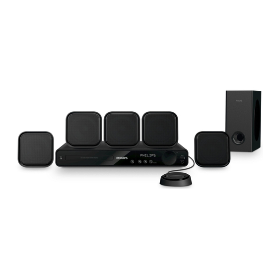
DVD Home Theatre System
©
Copyright 2009 Philips Consumer Electronics B.V. Eindhoven, The Netherlands
All rights reserved. No part of this publication may be reproduced, stored in a retrieval system or
transmitted, in any form or by any means, electronic, mechanical, photocopying, or otherwise
without the prior permission of Philips.
Published by
ET-SL 0906
Service Audio Printed in The Netherlands Subject to modification
Version 1.0
TABLE OF CONTENTS
Location of PCB Boards ............................................ 1-2
Versions Variation ...................................................... 1-2
Specifications ............................................................ 1-3
Measurement Setup .................................................. 1-4
Service Aids .............................................................. 1-5
ESD & Safety Instruction .......................................... 1-6
Lead-free soldering Information ................................ 1-7
Setting procedure & Repair Instructions........................ 2
Disassembly Instructions & Service positions .............. 3
Block & Wiring Diagram ................................................ 4
DISP+LED+VOL Board.................................................. 5
MAIN+Y.U.V Board ........................................................ 6
Power Board .................................................................. 7
MP3 IN Board ................................................................ 8
Mechanical Exploded View & Part List .......................... 9
Revision List ................................................................ 10
HTS3371D
Chapter
/F7
Made for
iPod
© 3141 785 33350
Advertisement
Table of Contents

Related Manuals for Philips HTS3371D


Summary of Contents for Philips HTS3371D
- Page 1 Revision List ..............10 © Copyright 2009 Philips Consumer Electronics B.V. Eindhoven, The Netherlands All rights reserved. No part of this publication may be reproduced, stored in a retrieval system or transmitted, in any form or by any means, electronic, mechanical, photocopying, or otherwise without the prior permission of Philips.
-
Page 2: Location Of Pcb Boards
LOCATION OF PCB BOARDS Y.U.V PCB MAIN PCB LED PCB DISPLAY PCB POWER PCB VOLUME PCB MP3 PCB VERSION VARIATION: Type/Versions HTS3371D Features Output Power - 1000W Voltage (120V) MP3 Link SERVICE SCNARIO MATRIX: HTS3371D Type/Versions Board in used MAIN+Y.U.V Board... -
Page 3: Specifications
PCM ................IEC 60958 Trade Name ..............Philips Dolby Digital .......... IEC 60958, IEC 61937 Responsible Party ..............Philips Consumer Lifestyle A Division of Philips Electronics Radio North America Corp. Tuning range ......... FM 87.5-108 MHz(100 kHz) P. O. Box 671539 2 6 dB quieting sensitivity ..........FM 22 dBf... - Page 4 1 - 4 MEASUREMENT SETUP Tuner FM Bandpass LF Voltmeter 250Hz-15kHz e.g. PM2534 e.g. 7122 707 48001 RF Generator e.g. PM5326 S/N and distortion meter e.g. Sound Technology ST1700B Use a bandpass filter to eliminate hum (50Hz, 100Hz) and disturbance from the pilottone (19kHz, 38kHz). Use Audio Signal Disc SBC429 4822 397 30184 (replaces test disc 3)
- Page 5 1 - 5 SERVICE AIDS Service Tools: Universal Torx driver holder .........4822 395 91019 Torx bit T10 150mm ...........4822 395 50456 Torx driver set T6-T20 .........4822 395 50145 Torx driver T10 extended ........4822 395 50423 Compact Disc: SBC426/426A Test disc 5 + 5A ......4822 397 30096 SBC442 Audio Burn-in test disc 1kHz ....4822 397 30155 SBC429 Audio Signals disc .........4822 397 30184 Dolby Pro-logic Test Disc ........4822 395 10216...
- Page 6 1 - 6...
- Page 7 1 - 7...
- Page 8 In open mode, press “1“ “5“ “9“ on R/C the software upgrade? b) Press “ok” button to con rm c) TV will show message as below: Cancel Current model HTS3371D/F7 Version: XX.XX.XX Release:XXXX.XX.XX f) Select “OK”, OSD will show: region Servo:XX.XX.XX.XX 8032:XX.XX.XX.XX...
- Page 9 2 - 2 2 - 2 REPAIR INSTRUCTIONS (ONE)
- Page 10 2 - 3 2 - 3 REPAIR INSTRUCTIONS (TWO)
- Page 11 2 - 4 2 - 4 REPAIR INSTRUCTIONS (THREE)
- Page 12 3 - 1 3 - 1 DISASSEMBLY INSTRUCTIONS Dismantling of the Front Panel Assemble 3) Loosen 6 screws and remove the Top Cover by lifting the rear portion upwards before sliding it out towards the rear. - 1 screw “A” each on the left & right side as shown in gure 4. 1) Open the DVD Tray by using the Open/Close Button while the Set is ON and disconnect the mains supply after removing the Tray - 4 screws “B”...
-
Page 13: Service Positions
3 - 2 3 - 2 Dismantling of the DISP+LED+VOL&MP3 IN Board SERVICE POSITIONS 1) Loosen 10 screws “E” on the top of DISP+LED+VOL&MP3 IN Board as shown in gure 8. Service position A Figure 8 Dismantling of the Power Board 1) Loosen 4 screws “F”... -
Page 14: Block Diagram
4 - 1 4 - 1 BLOCK DIAGRAM Sanyo / Sony pick up VF D Display AS A DVD Loader B+5V IC V 5888 V- CL K VF D DR IV ER V- CS PT6311 Loader motor driver V- DAT A KE Y 1080P 3.3V... - Page 15 4 - 2 4 - 2 WIRING DIAGRAM...
-
Page 16: Disp+Led+Vol Board
5 - 1 5 - 1 FTD DISPLAY PIN ASSIGNMENT DISP+LED+VOL BOARD TABLE OF CONTENTS FTD Display Pin Assignment ............. 5-1 Circuit Diagram ................. 5-2 PCB Layout Top & Bottom View ............5-3 PIN CONNECTION... - Page 17 5 - 2 5 - 2 CIRCUIT DIAGRAM C380 B1 C384 C1 C387 A2 C390 B2 C395 C4 DP351 A2 Q351 C1 R3051 B1 R3054 B1 R3057 C1 R3060 C1 R3063 B1 R3068 A3 R3072 C1 RB351 C4 RB357 C1 TA351 A1 TA354 C1 ZD310 C1...
- Page 18 5 - 3 5 - 3 PCB LAYOUT - TOP VIEW C386 C391 DP351 A2 ESD4 ESD6 J351 J353 J355 J357 J359 LD351 RB355 A1 RB357 B1 SN351 B3 TA352 TA354 VR351 A3 C389 C392 ESD1 ESD5 ESD7 J352 J354 J356 J358 J363...
-
Page 19: Table Of Contents
6 - 1 6 - 1 INTERNAL IC DIAGRAM - TAS5508B MAIN BOARD TABLE OF CONTENTS Internal IC Diagram ................6-1 Circuit Diagram(part one) ..............6-2 Circuit Diagram(part two) ..............6-3 Circuit Diagram(part three) ..............6-4 PCB Layout Top View ............... 6-5 PCB Layout Bottom View .............. -
Page 20: Circuit Diagram(Part One)
6 - 2 6 - 2 CIRCUIT DIAGRAM - part one C4000 B4 C4010 B3 C4023 B4 C4035 A4 C4045 A4 C407 B1 C409 B1 C421 B1 C434 D3 C447 D4 C460 D4 C471 B3 C484 C4 C497 B4 D410 D2 IC406 D2 L409 B4 Q407 D1... -
Page 21: Circuit Diagram(Part Two)
6 - 3 6 - 3 CIRCUIT DIAGRAM - part two C0201 C2 C0217 D1 C0241 D4 C0606 C4 C211 C229 C1 C260 D1 C711 C737 C817 C833 CE204 D1 CE806 D1 CO254 A2 FB210 C1 FB706 A3 IC209 B3 L703 Q707 A3 R211... -
Page 22: Circuit Diagram(Part Three)
6 - 4 6 - 4 CIRCUIT DIAGRAM - part three C301 A1 C313 A2 C324 B3 C334 B2 C351 B3 C366 A1 C515 B4 C908 D2 C932 D1 CE309 D2 CE319 D2 CE329 D3 CE904 D1 FE302 D3 IC304 A2 Q305 A3 R3020 B2 R311 A1... -
Page 23: Pcb Layout Top View
6 - 5 6 - 5 PCB LAYOUT - TOP VIEW C0202 A2 C214 C1 C261 C2 C342 B3 C4012 C4 C4072 A3 C442 B4 C490 C4 C716 A1 C818 D1 C912 C2 CN208 D2 FB210 D2 FB802 D1 IC402 C4 L403 L704 Q804 D1... -
Page 24: Pcb Layout Bottom View
6 - 6 6 - 6 PCB LAYOUT - BOTTOM VIEW C0201 C4 C0218 B3 C0241 A1 C206 B4 C308 A3 C4002 A2 C4039 B2 C409 D1 C446 B1 C469 B1 C511 C2 C802 D4 C904 D2 CE215 A4 CE309 D2 CE323 B3 CE804 D3 D414 A2... -
Page 25: Power Board
7 - 1 7 - 1 INTERNAL IC DIAGRAM - AZ431 CATHODE POWER BOARD TABLE OF CONTENTS Internal IC Diagram ................7-1 Circuit Diagram .................. 7-2 ANODE PCB Layout Top View ............... 7-3 PCB Layout Bottom View ..............7-4... - Page 26 7 - 2 7 - 2 CIRCUIT DIAGRAM BD901 A1 C910 D3 C923 D2 C936 B2 C947 C3 C957 A4 C965 C3 C974 B4 C985 B3 D904 B4 D914 A4 D924 A3 IC905 B4 L908 A3 Q911 B3 R904 C1 R914 C1 R924 A3 R933 C2...
- Page 27 7 - 3 7 - 3 PCB LAYOUT - TOP VIEW BD901 B1 C906 A3 C920 A2 C959 A3 C966 B4 C975 C4 CN906 C4 D917 B2 D927 B4 IC905 B4 J906 C2 J912 A4 J919 A4 J925 C4 L901 D4 L908 C4 Q914 A3 R940 B2...
- Page 28 7 - 4 7 - 4 PCB LAYOUT - BOTTOM VIEW C907 B1 C928 A1 C938 A2 C947 B2 C955 B1 C967 B2 C983 B2 D904 B1 D916 C2 Q906 A2 R904 D4 R909 C1 R918 A3 R925 A2 R933 A3 R938 B2 R954 A2 R964 B1...
-
Page 29: Mp3 In Board
8 - 1 8 - 1 MP3 IN BOARD TABLE OF CONTENTS Circuit Diagram .................. 8-1 PCB Layout Top & Bottom View ............8-2... - Page 30 8 - 2 8 - 2 CIRCUIT DIAGRAM C383 A3 FB351 A1 FB352 A1 FB355 A3 FB356 A3 FB357 A3 JK351 A2 R3079 A1 R3080 A1 RB352 A1 RB354 A2 USB351 A3 RB352 JK 351 FB 351 C383 MP3L USB 351 R 3079 RB354 FB 355...
- Page 31 8 - 3 8 - 3 PCB LAYOUT - TOP VIEW PCB LAYOUT - BOTTOM VIEW J360 J361 JK351 RB352 A1 RB354 A1 USB351 A2 C383 FB351 FB352 FB355 FB356 FB357 R3079 R3080...
- Page 32 9 - 1 9 - 1 Mechanical Exploded View A1=11+10+18 A2=30+35...
- Page 33 IC402 996510021081 IC 44P TAS5352ADDV HTSSOP TI SPKC 996510021124 SPEAKER BOX-CENTER IC905 996510008293 IC 16P AZ7500BP-E1 IC407 996500023948 IC 14P 74HCU04D PHILIPS TSOP SPKFL SPKFL 996510021123 996510021123 SPEAKER BOX-FRONT LEFT SPEAKER BOX-FRONT LEFT L901 L901 996510021083 996510021083 COMMON COIL 6mH 21 5Ts D0 6mm COMMON COIL 6mH 21.5Ts D0.6mm...
-
Page 34: Revision List
10 - 1 10 - 1 REVISION LIST Version 1.0 *Initial release...