Table of Contents
Advertisement
Quick Links
D-EJ750/EJ751/EJ753/EJ755/EJ756CK/EJ758CK
QQ
3 7 63 1515 0
SERVICE MANUAL
Ver 1.0 2002.02
TE
L 13942296513
System
Compact disc digital audio system
Laser diode properties
Material: GaAlAs
Wavelength : λ = 780 nm
Emission duration : Continuous
Laser output : Less than 44.6 µW
(This output is the value measured at a distance
of 200 mm from the objective lens surface on
the optical pick-up block with 7 mm aperture.)
D-A conversion
1-bit quartz time-axis control
Frequency response
+1
20 - 20 000 Hz
dB (measured by JEITA CP-307)
–2
Output (at 4.5 V input level)
Line output (stereo minijack)
Output level 0.7 V rms at 47 k
Recommended load impedance over 10 k
Headphones (stereo minijack)
Approx.5 mW + Approx. 5 mW at 16 Ω
(Approx. 0.5 mW + Approx. 0.5 mW at 16 Ω)*
*For the customers in France
Power requirements
For the area code of the model you
purchased, check the upper left side of the
bar code on the package.
• Two Sony NC-WMAA rechargeable
batteries: 2.4 V DC
• Sony NH-WM2AA rechargeable batteries:
2.4 V DC
• Two LR6 (size AA) batteries: 3 V DC
• AC power adaptor (DC IN 4.5 V jack):
www
US, CND, C&SA, MX model: 120 V, 60 Hz
AEP, FR, G, EE, E13 mode : 220 - 230 V, 50/60 Hz
UK model: 230 - 240 V, 50 Hz
AUS model: 240 V, 50 Hz
CH model: 220 V, 50 Hz
.
Sony Corporation
9-873-580-01
2002B0200-1
Personal Audio Company
© 2002.02
Pubulished by Sony Engineering Corporation
http://www.xiaoyu163.com
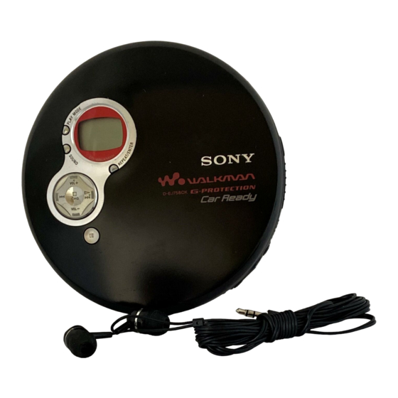
Photo : D-EJ755
Battery life* (approx. hours)
(When you use the CD player on a flat and stable sur-
face.)
Playing time varies depending on how the CD player is
used.
When using
Two NC-WMAA
(charged for
about 3 hours**)
NH-WM2AA
(charged for
about 5 hours**)
Two Sony alkaline
batteries LR6(SG)
(produced in Japan)
* Measured value by the standard of JEITA (Japan
Electronics and Information Technology
Industries Association).
** Charging time varies depending on how the
rechargeable battery is used.
Operating temperature
5°C - 35°C (41°F - 95°F)
Dimensions (w/h/d) (excluding projecting
parts and controls)
Approx. 135.5 × 29.2 × 137.4 mm
× 1
3
(5
⁄
8
Mass (excluding accessories)
Approx. 185 g (6.6 oz.)
Design and specifications are subject to change
x
ao
u163
without notice.
y
i
http://www.xiaoyu163.com
2 9
8
Model Name Using Similar Mechanism D-E350
CD Mechanism Type
Optical Pick-up Type
Q Q
SPECIFICATIONS
3
6 7
1 3
1 5
G-PROTECTION function
on
off
12
10
25
22
48
38
× 5
3
1
⁄
⁄
in.)
16
2
co
.
9 4
2 8
US Model
D-EJ756CK/EJ758CK
Canadian Model
UK Model
D-EJ751/EJ755/EJ758CK
AEP Model
D-EJ750/EJ751/EJ753/EJ755/EJ758CK
Australian Model
E Model
D-EJ751/EJ758CK
Chinese Model
CDM-3125ER
DAX-25E
0 5
8
2 9
9 4
2 8
Accessories
Supplied accessories
For the area code of the location in which you
purchased the CD player, check the upper left
side of the bar code on the package.
–
AC power adaptor (1)
–
Headphones/earphones
with remote control (1)
Headphones/
a
earphones (1)
–
Rechargeable
batteries (2)
–
Battery carrying case (1)
* 1 Supplied with MX models
* 2 Not supplied with MX models
D-EJ756CK/EJ758CK
AC power adaptor (1)
Headphones/earphones (1)
Rotary commander (1)
Car battery cord (1)
Car connecting pack (1)
Velcro tape for the CD player (4)
Velcro tape for the rotary commander (2)
Hand strap (1)
m
PORTABLE CD PLAYER
9 9
D-EJ751
9 9
a
a
a
1
*
a
a
–
2
*
a
a
–
a
a
–
a
a
Advertisement
Table of Contents

Related Manuals for Sony D-EJ750


Summary of Contents for Sony D-EJ750
-
Page 1: Specifications
5°C - 35°C (41°F - 95°F) bar code on the package. Car battery cord (1) Dimensions (w/h/d) (excluding projecting • Two Sony NC-WMAA rechargeable Car connecting pack (1) parts and controls) batteries: 2.4 V DC Velcro tape for the CD player (4) Approx. -
Page 2: Table Of Contents
DIAGRAMMES SCHÉMATIQUES ET LA LISTE DES PIÈCES SONT CRITIQUES POUR LA SÉCURITÉ DE FONCTIONNEMENT. NE REMPLACER CES COMPOSANTS QUE PAR DES PIÈCES SONY DONT LES NUMÉROS SONT DONNÉS DANS CE MANUEL OU DANS LES SUPPLÉMENTS PUBLIÉS PAR SONY. u163 http://www.xiaoyu163.com... -
Page 3: Servicing Notes
D-EJ750/EJ751/EJ753/EJ755/EJ756CK/EJ758CK SECTION 1 3 7 63 1515 0 SERVICING NOTES Laser Diode Checking Methods NOTES ON HANDLING THE OPTICAL PICK-UP BLOCK OR During normal operation of the equipment, emission of the laser diode BASE UNIT is prohibited unless the upper panel is closed while turning ON the S801 (push switch type). -
Page 4: Disassembly
D-EJ750/EJ751/EJ753/EJ755/EJ756CK/EJ758CK SECTION 3 3 7 63 1515 0 DISASSEMBLY The equipment can be removed using the following procedure. MD ASSY “Motor ASSY, turn table (spindle) (M901)”, Optical pick-up (DAX-25E), Upper lid sub ASSY, “Motor ASSY (Sled) (M902)” Cabinet (front) sub ASSY Main board Note : Follow the disassembly procedure in the numerical order given. -
Page 5: Md Assy, Main Board
D-EJ750/EJ751/EJ753/EJ755/EJ756CK/EJ758CK 3 7 63 1515 0 3-2. MD ASSY, MAIN BOARD MD ASSY 1 CN501 2 CN502 (black) 3 CN503 (white) Main board Cabinet (rear) sub ASSY L 13942296513 3-3. “MOTOR ASSY, TURN TABLE (SPINDLE) (M901)” 1 Screws (B1.7x5) -
Page 6: Motor Assy (Sled) (M902)
D-EJ750/EJ751/EJ753/EJ755/EJ756CK/EJ758CK 3 7 63 1515 0 3-4. “MOTOR ASSY (SLED) (M902)”, OPTICAL PICK-UP (DAX-25E) 1 Screw (B 1.7x5) Cover, Gear Gear B Screw ASSY, Feed Motor ASSY (Sled) (M902) 4 Screw (P 1.4x3.5) Bracket (Shaft) Optical pick-up (DAX-25E) Chassis... -
Page 7: Electrical Adjustmens
D-EJ750/EJ751/EJ753/EJ755/EJ756CK/EJ758CK SECTION 4 3 7 63 1515 0 ELECTRICAL ADJUSTMENTS The CD section adjustments are done automatically in this set. Focus bias Check Condition: Precautions for Check • Hold the set in horizontal state. 1. Perform check in the order given. -
Page 8: Diagrams
D-EJ750/EJ751/EJ753/EJ755/EJ756CK/EJ758CK SECTION 5 DIAGRAMS 3 7 63 1515 0 5-1. EXPLANATION OF IC TERMINALS IC601 (SYSTEM CONTROL) CXD3029R (DSP IC) Pin No. Pin name Description XRAM DRAM low address strobe signal outut. DRAM data input enable signal output. 3 to 6 D0 to 3 DRAM data bus 0 to 3. - Page 9 D-EJ750/EJ751/EJ753/EJ755/EJ756CK/EJ758CK 3 7 63 1515 0 Pin No. Pin name Description VREFR VREF terminal(R-CH). AOUT2 Line out. – Power supply terminal for analog. TEST1 Not used (Fixed at “L”). TEST Not used (Fixed at “L”).. Vss1 – Not used (Fixed at “L”).
- Page 10 D-EJ750/EJ751/EJ753/EJ755/EJ756CK/EJ758CK 3 7 63 1515 0 Pin No. Pin name Description – Power supply terminal for digital. LRCK LR clock output for D/A interface. LRCKI LR clock input for D/A interface. PCMD Serial data output for D/A interface. PCMDI Serial data input for D/A interface.
- Page 11 D-EJ750/EJ751/EJ753/EJ755/EJ756CK/EJ758CK 3 7 63 1515 0 IC801 (SYSTEM CONTROL) T5AW5-NJR2-M1 Pin No. Pin name Description – Ground terminal. System clock input (4.19MHz). XOUT System clock output (4.19MHz). TEST Test mode terminal (Fixed to “L”). VCPU – Power supply for CPU & I/O.
- Page 12 D-EJ750/EJ751/EJ753/EJ755/EJ756CK/EJ758CK 3 7 63 1515 0 Pin No. Pin name Description SO_O Serial data clock output. PGMSI_I Serial date input. PGMSCK_O Serial data output. AGCPWM_O PWM output for laser AGC. IR_RMC_I Not used (Fixed to “H”). FG_I/FGSEL_I FG input / spindle motor select.
-
Page 13: Block Diagram
D-EJ750/EJ751/EJ753/EJ755/EJ756CK/EJ758CK 3 7 6 3 1 5 1 5 0 5-2. BLOCK DIAGRAM US MODEL EXCEPT US MODEL IC602 IC603 J301 RAM(16M) RAM(4M) AOUT1 LINE AOUT2 D0-3 A0-10 D0-3 A0-9 MUTE 2,3,24,25 8-12,15-19,21 5 23 4 1,2,24,25 5,9-12,14-19 4 23 3... -
Page 14: Printed Wiring Boards
D-EJ750/EJ751/EJ753/EJ755/EJ756CK/EJ758CK 3 7 6 3 1 5 1 5 0 5-3. PRINTED WIRING BOARDS MAIN BOARD MAIN BOARD (SIDE B) (SIDE A) DC IN 4.5V DRY BATTERY SIZE "AA" (IEC DESIGNATION LR6) 2PCS, 3V RECHARGEABLE BATTERY NC–WMAA/NH–WM2AA 2.4V 1 3 9 4 2 2 9 6 5 1 3... -
Page 15: Schematic Diagram -Main Section (1/3)
D-EJ750/EJ751/EJ753/EJ755/EJ756CK/EJ758CK 3 7 6 3 1 5 1 5 0 5-4. SCHEMATIC DIAGRAM – MAIN SECTION (1/3) – • Refer to page 18 for Notes. • Refer to page 18 for waveforms. • Refer to page 18 for IC Block diagram. -
Page 16: Schematic Diagram -Main Section (2/3)
D-EJ750/EJ751/EJ753/EJ755/EJ756CK/EJ758CK 3 7 6 3 1 5 1 5 0 5-5. SCHEMATIC DIAGRAM – MAIN SECTION (2/3) – • Refer to page 18 for Notes. 1 3 9 4 2 2 9 6 5 1 3 w w w u 1 6 3 http://www.xiaoyu163.com... -
Page 17: Schematic Diagram -Main Section (3/3)
D-EJ750/EJ751/EJ753/EJ755/EJ756CK/EJ758CK 3 7 6 3 1 5 1 5 0 5-6. SCHEMATIC DIAGRAM – MAIN SECTION (3/3) – • Refer to page 18 for Notes. 1 3 9 4 2 2 9 6 5 1 3 w w w u 1 6 3 http://www.xiaoyu163.com... - Page 18 D-EJ750/EJ751/EJ753/EJ755/EJ756CK/EJ758CK 3 7 6 3 1 5 1 5 0 Waveforms Note: • All capacitors are in µF unless otherwise noted. pF: µµF 50 WV or less are not indicated except for electrolytics and tantalums. • All resistors are in Ω and W or less unless otherwise specifed.
-
Page 19: Exploded Views
D-EJ750/EJ751/EJ753/EJ755/EJ756CK/EJ758CK SECTION 6 3 7 63 1515 0 EXPLODED VIEWS NOTE : • -XX, -X mean standardized parts, so they • The mechanical parts with no reference The components identified by mark 0 may have some difference from the original... -
Page 20: Q Q 6-2. Cabinet Section
D-EJ750/EJ751/EJ753/EJ755/EJ756CK/EJ758CK 3 7 63 1515 0 6-2. CABINET SECTION not supplid L 13942296513 Ref. No. Part No. Description Remark Ref. No. Part No. Description Remark 3-235-304-01 LID, BATTERY CASE...(SILVER, BLUE) X-3381-369-1 CABINET (REAR) SUB ASSY...(SILVER, BLUE) 3-235-304-11 LID, BATTERY CASE...(YELLOW) X-3381-371-1 CABINET (REAR) SUB ASSY...(YELLOW) -
Page 21: Optical Pick-Up Section (Cdm-3125Er)
D-EJ750/EJ751/EJ753/EJ755/EJ756CK/EJ758CK 3 7 63 1515 0 6-3. OPTICAL PICK-UP SECTION (CDM-3125ER) M901 L 13942296513 M902 The components identified by Les composants identifiés par une mark 0 or dotted line with mark marque 0 sont critiques pour 0 are critical for safety. -
Page 22: Electrical Parts List
D-EJ750/EJ751/EJ753/EJ755/EJ756CK/EJ758CK SECTION 7 MAIN ELECTRICAL PARTS LIST 3 7 63 1515 0 NOTE : • Due to standardization, replacements in the • SEMICONDUCTORS In each case, u : µ , for example : The components identified by mark 0... - Page 23 D-EJ750/EJ751/EJ753/EJ755/EJ756CK/EJ758CK MAIN 3 7 63 1515 0 Ref. No. Part No. Description Remark Ref. No. Part No. Description Remark C606 1-164-156-11 CERAMIC CHIP 0.1uF D306 8-719-084-06 DIODE MM3Z5VT1 C607 1-162-923-11 CERAMIC CHIP 47PF D401 8-719-085-43 DIODE MA2YD2300LS0 C608 1-164-346-11 CERAMIC CHIP...
- Page 24 D-EJ750/EJ751/EJ753/EJ755/EJ756CK/EJ758CK MAIN 3 7 63 1515 0 Ref. No. Part No. Description Remark Ref. No. Part No. Description Remark <TRANSISTOR> R421 1-216-857-11 METAL CHIP 1/16W R422 1-216-833-11 METAL CHIP 1/16W Q301 8-729-427-72 TRANSISTOR XP4501 R423 1-216-837-11 METAL CHIP 1/16W...
- Page 25 D-EJ750/EJ751/EJ753/EJ755/EJ756CK/EJ758CK MAIN 3 7 63 1515 0 Ref. No. Part No. Description Remark Ref. No. Part No. Description Remark R639 1-216-837-11 METAL CHIP 1/16W <VIBLATOR> R640 1-216-845-11 METAL CHIP 100K 1/16W X601 1-795-101-21 VIBRATOR, CERAMIC (16.9MHz) R801 1-216-845-11 METAL CHIP...
- Page 26 D-EJ750/EJ751/EJ753/EJ755/EJ756CK/EJ758CK 3 7 63 1515 0 Ref. No. Part No. Description Remark 3-237-145-31 MANUAL, INSTRUCTION (EJ751:CH) (SIMPLIFIED CHINESE) 3-237-146-11 MANUAL, INSTRUCTION (EJ750:EE/EJ751:EE/ EJ755:EE) (RUSSIAN) 3-237-146-21 MANUAL, INSTRUCTION (EJ750:EE/EJ751:EE/ EJ755:EE) (CZECH) 3-237-146-31 MANUAL, INSTRUCTION (EJ750:EE/EJ751:EE/ EJ755:EE) (HUNGARIAN) 3-237-146-41 MANUAL, INSTRUCTION (EJ750:EE/EJ751:EE/...
- Page 27 D-EJ750/EJ751/EJ753/EJ755/EJ756CK/EJ758CK 3 7 63 1515 0 L 13942296513 u163 http://www.xiaoyu163.com...
- Page 28 D-EJ750/EJ751/EJ753/EJ755/EJ756CK/EJ758CK 3 7 63 1515 0 REVISION HISTORY Clicking the version allows you to jump to the revised page. Also, clicking the version at the upper right on the revised page allows you to jump to the next revised page.