Table of Contents
Advertisement
SERVICE MANUAL
Ver 1.0 2004.03
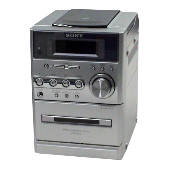
• HCD-NE3 is the amplifier, CD player, tape deck
and tuner section in CMT-NE3.
AUDIO POWER SPECIFICATIONS
POWER OUTPUT AND TOTAL HARMONIC
DISTORTION:
(US model)
With 6 ohm loads, both channels driven, from
120-10,000 Hz; rated 13 watts per channel
minimum RMS power, with no more than 10%
total harmonic distortion from 250 milliwatts to
rated output.
Main unit
Amplifier section
North American model:
Continuous RMS power output (reference):
15 + 15 W
(6 ohms at 1 kHz, 10%
THD)
European model:
DIN power output (rated): 11 + 11 W (6 ohms at 1
kHz, DIN)
Continuous RMS power output (reference):
15 + 15W (6 ohms at 1
kHz, 10% THD)
Music power output (reference):
25 + 25 W
Other models:
The following measured at AC 230 V or AC 120 V, 50/
60 Hz
DIN power output (rated): 11 + 11 W
(6 ohms at 1 kHz, DIN)
Continuous RMS power output (reference):
15 + 15 W
(6 ohms at 1 kHz, 10%
THD)
Sony Corporation
9-877-693-01
2004C05-1
Home Audio Company
© 2004.03
Published by Sony Engineering Corporation
CD Section
TAPE Section
SPECIFICATIONS
Inputs
MD (phono jacks):
Sensitivity 450 mV,
impedance 47 kilohms
Outputs
PHONES:
Accepts headphones with
an impedance of 8 ohms or
more
SPEAKER:
Accepts impedance of 6 to
16 ohms.
CD player section
Laser
Semiconductor laser
(λ=780 nm)
Emission duration:
continuous
Frequency response
20 Hz – 20 kHz
Wavelength
780 – 790 nm
Tape deck section
Recording system
4-track 2-channel, stereo
Frequency response
50 – 13,000 Hz (±3 dB),
using Sony TYPE I
cassettes
HCD-NE3
Model Name Using Similar Mechanism
Base Unit Name
Optical Pick-up Name
Model Name Using Similar Mechanism
Tape Transport Mechanism Type
Tuner section
FM stereo, FM/AM superheterodyne tuner
FM tuner section
Tuning range
87.5 – 108.0 MHz
Antenna
FM lead antenna
Antenna terminals
75 ohms unbalanced
Intermediate frequency
10.7 MHz
AM tuner section
US, Canadian, Mexican and Argentina models:
530 – 1,710 kHz
(with the tuning interval
set at 10 kHz)
531 – 1,710 kHz
(with the tuning interval
set at 9 kHz)
AEP and UK models:
531 – 1,602 kHz
(with the tuning interval
set at 9 kHz)
Other models:
530 – 1,710 kHz
(with the tuning interval
set at 10 kHz)
531 – 1,602 kHz
(with the tuning interval
set at 9 kHz)
Antenna
AM loop antenna, external
antenna terminal
Intermediate frequency
450 kHz
COMPACT DISC DECK RECEIVER
US Model
Canadian Model
AEP Model
UK Model
E Model
Australian Model
NEW
BU-K7BD80B
KSM-213EDP/C2NP
NEW
CMAL5Z220A
General
Power requirements
US, Canadian and Mexican models:
120 V AC, 60 Hz
AEP and UK models:
230 V AC, 50/60 Hz
Australian model:
230 – 240 V AC, 50/60 Hz
Argentina and Korean models:
220 V AC, 60 Hz
Taiwanese model:
120 V AC, 50/60 Hz
Saudi Arabian model:
120 – 127/220 V AC, 50/
60 Hz
Other models:
110 – 120 V or 220 – 240 V
AC, 50/60 Hz
Adjustable with voltage
selector
Power consumption
45 W
Approx. 164 × 230.5 × 263
Dimensions (w/h/d)
mm incl. projecting parts
and controls
Mass
Approx. 3.7 kg
Supplied accessories
Remote Commander (1)
R6 (size AA) batteries (2)
AM loop antenna (1)
FM lead antenna (1)
Design and specifications are subject to change
without notice.
Advertisement
Table of Contents

Related Manuals for Sony HCD-NE3


Summary of Contents for Sony HCD-NE3
-
Page 1: Specifications
Canadian Model Ver 1.0 2004.03 AEP Model UK Model E Model Australian Model • HCD-NE3 is the amplifier, CD player, tape deck and tuner section in CMT-NE3. Model Name Using Similar Mechanism CD Section Base Unit Name BU-K7BD80B Optical Pick-up Name... -
Page 2: Leakage Test
OPERATION. REPLACE THESE COMPONENTS WITH DE FONCTIONNEMENT. NE REMPLACER CES COM- SONY PARTS WHOSE PART NUMBERS APPEAR AS POSANTS QUE PAR DES PIÈCES SONY DONT LES SHOWN IN THIS MANUAL OR IN SUPPLEMENTS PUB- NUMÉROS SONT DONNÉS DANS CE MANUEL OU LISHED BY SONY. -
Page 3: Table Of Contents
HCD-NE3 TABLE OF CONTENTS SERVICING NOTES ..........4 GENERAL Location of Controls ............6 DISASSEMBLY 3-1. Disassembly Flow ............8 3-2. Rear Cabinet ..............8 3-3. Top Panel Assy ..............9 3-4. Front Panel Assy ............. 9 3-5. Base Unit (BU-K7BD80B) ..........10 3-6. -
Page 4: Servicing Notes
HCD-NE3 SECTION 1 SERVICING NOTES • MODEL IDENTIFICATION NOTES ON HANDLING THE OPTICAL PICK-UP – Rear Cabinet – BLOCK OR BASE UNIT The laser diode in the optical pick-up block may suffer electro- static break-down because of the potential difference generated by the charged electrostatic load, etc. - Page 5 HCD-NE3 SERVICE POSITION – BD board – BD board – TCM block – TCM block – AMP board – AMP board...
-
Page 6: General
HCD-NE3 SECTION 2 This section is extracted from instruction manual. GENERAL • LOCATION OF CONTROLS Main unit ALPHABETICAL ORDER BUTTON DESCRIPTIONS ?/1 (power) 1 P – Z A – O .m/M> (skip back/ PHONES jack qk BASS/TREBLE 8 skip forward,rewind/fast... -
Page 7: Setting The Clock
HCD-NE3 Setting the clock Remote control ALPHABETICAL ORDER BUTTON DESCRIPTIONS Use buttons on the remote for the operation. ?/1 (power) 1 A – O P – Z Press ?/1 to turn on the system. m/M (rewind/fast forward) CD qh PLAY MODE qk Press CLOCK/TIMER SET. -
Page 8: Disassembly
HCD-NE3 SECTION 3 DISASSEMBLY • This set can be disassembled in the order shown below. 3-1. DISASSEMBLY FLOW 3-2. REAR CABINET (Page 8) 3-3. TOP PANEL ASSY (Page 9) 3-4. FRONT PANEL ASSY 3-5. BASE UNIT (Page 9) (BU-K7BD80B) (Page 10) 3-6. -
Page 9: Top Panel Assy
HCD-NE3 3-3. TOP PANEL ASSY 6 top panel assy 5 connector (S820) 4 wire (flat type) (17 core) (CN305) 2 claw 1 claw 3-4. FRONT PANEL ASSY 2 wire (flat type) (8 core) (CN303) q; wire (flat type) (11 core) -
Page 10: Base Unit (Bu-K7Bd80B)
HCD-NE3 3-5. BASE UNIT (BU-K7BD80B) 6 base unit (BU-K7BD80B) 4 two screws (2.6 × 10) 5 two screws (2.6 × 10) 3 wire (flat type) (17core) (CN201) 2 CD cover 1 three screws (BVTP2.6 × 8) 3-6. MECHANICAL DECK 1 three screws 2 screw (2.6 ×... -
Page 11: Main Board
HCD-NE3 3-7. MAIN BOARD 5 main board 1 connector (CNB308) 3 connector (CNB307) 4 two screws (BVTP3 × 10) 6 tuner (FM/AM) 2 connector (CN902) 3-8. AMP BOARD 4 AMP board 3 two screws (BVTP3 × 10) 1 connector (CNB308) -
Page 12: Test Mode
(In this case, North-American model) Search operation is under way model name Playback operation is under way (In this case, HCD-NE3) Pause operation is under way To exit from this mode, perform the “COLD RESET”. Playback manual search operation is under way... - Page 13 HCD-NE3 TUNER STEP CHANGE-OVER Either the 9 kHz step or 10 kHz step can be selected for the AM channel step. Procedure: 1. Set the FUNCTION to AM, and press the button to turn the power off. 2. While depressing the button, press TUNING + M >...
-
Page 14: Electrical Check
HCD-NE3 SECTION 5 ELECTRICAL CHECK Note: CD Block is basically constructed to operate without adjustment. Use YEDS-18 disc (3-702-101-01) unless otherwise indicated. Use an oscilloscope with more than 10 MΩ impedance. Clean the object lens by an applicator with neutral detergent when the signal level is low than specified value with the following checks. -
Page 15: Diagrams
HCD-NE3 SECTION 6 DIAGRAMS 6-1. BLOCK DIAGRAM – CD SERVO Section – FILTER XTSL CD DSP XTAO IC101 (1/2) CLOCK X171 48 50 47 49 DETECTOR D +3.3V XTAI GENERATOR 16.9344MHz XTACN RFACO RFACI AOUT1 RFAC ASYMMETRY (Page 16) SUMMING... -
Page 16: Block Diagram - Main Section
HCD-NE3 6-2. BLOCK DIAGRAM – MAIN Section – J303 19 AUX-L R-CH OUT-L POWER J301 PHONES (Page 15) IC501 21 CD-L R-CH • R-ch is omitted due to same as L-ch. FM/AM TUNER PACK • SIGNAL PATH FM 75Ω FM ANT... -
Page 17: Note For Printed Wiring Boards And Schematic Diagrams
HCD-NE3 6-3. NOTE FOR PRINTED WIRING BOARDS AND SCHEMATIC DIAGRAMS • Circuit Boards Location Note on Printed Wiring Board: Note on Schematic Diagram: • All capacitors are in µF unless otherwise noted. pF: µµF • X : parts extracted from the component side. -
Page 18: Printed Wiring Board - Bd Board
HCD-NE3 PRINTED WIRING BOARD – BD Board – • 6-4. :Uses unleaded solder. See page 17 for Circuit Boards Location. BD BOARD C116 JW118 C123 JR109 C122 C117 JR108 OPTICAL R131 R121 JR105 R111 R112 JR111 PICK-UP C131 JW114 C111... -
Page 19: Schematic Diagram - Bd Board
HCD-NE3 SCHEMATIC DIAGRAM – BD Board – • • 6-5. See page 28 for IC Block Diagrams. See page 28 for Waveforms. CN201 XTACN TP29 XTACN C201 C182 C181 AGND DOUT TP31 DOUT R161 AVDD R201 TP32 AVDD LOUT TP33... -
Page 20: Printed Wiring Boards - Main Section
HCD-NE3 PRINTED WIRING BOARDS – MAIN Section – • 6-6. See page 17 for Circuit Boards Location. :Uses unleaded solder. • Semiconductor Location BD BOARD AMP BOARD CONTROL BOARD Ref. No. Location CN201 CN502 CNB303 (Page 18) (Page 22) (Page 24) -
Page 21: Schematic Diagram - Main Section
HCD-NE3 SCHEMATIC DIAGRAM – MAIN Section – • • 6-7. See page 28 for IC Block Diagram. See page 28 for Waveforms. J302 C119 R225 C232 0.01 SPEAKER R136 IMPEDANCE R125 C132 USE 8-16 C219 C117 0.0012 R126 C136 TU LCH 0.01... -
Page 22: Printed Wiring Boards - Amp Section
HCD-NE3 PRINTED WIRING BOARDS – AMP Section – • 6-8. :Uses unleaded solder. See page 17 for Circuit Boards Location. MAIN BOARD CNB308 AMP BOARD HP BOARD (Page 20) MAIN BOARD CN309 (Page 20) R517 R518 CNB501 CN502 J301 CN501... -
Page 23: Schematic Diagram - Amp Section
HCD-NE3 6-9. SCHEMATIC DIAGRAM – AMP Section – CN502 R515 R516 PROTECT R514 AMP-STBY C512 C514 R507 R512 AMP-MUTE (Page 21) C511 C513 AGND C516 C506 CN501 R517 R519 R501 R506 R508 SP OUT(R) R502 R505 HP OUT(R) HP OUT(L) -
Page 24: Printed Wiring Boards - Panel Section
HCD-NE3 6-10. PRINTED WIRING BOARDS – PANEL Section – • :Uses unleaded solder. See page 17 for Circuit Boards Location. • Semiconductor Location Ref. No. Location CONTROL BOARD BACK LIGHT D701 CNB302 BOARD D702 JR107 D703 R712 D801 LCD801 JR106... -
Page 25: Schematic Diagram - Panel Section
HCD-NE3 6-11. SCHEMATIC DIAGRAM – PANEL Section – • • See page 28 for Waveforms. See page 30 for IC Pin Function Description. LCD801 LIQUID CRYSTAL DISPLAY D701-703 R707 (LCD BACK LIGHT) D701 SELS6B14CS-TP5 R708 CNB806 CNB807 R709 BLT- D702 C803 0.01... -
Page 26: Printed Wiring Board - Power Board
HCD-NE3 6-12. PRINTED WIRING BOARD – POWER Board – • See page 17 for Circuit Boards Location. :Uses unleaded solder. • Semiconductor Location Ref. No. Location D906 POWER BOARD D907 D908 (EXCEPT E, E51, EA, SP) D909 (E, E51, EA, SP) -
Page 27: Schematic Diagram - Power Board
HCD-NE3 6-13. SCHEMATIC DIAGRAM – POWER Board – T902 MAIN POWER C907 D918 D916 TRANSFORMER 0.022 1N5401M 1N5401M C908 D919 D917 D920 R901 0.022 1N5401M 1N5401M 1SS133T-77 D921 R902 C902 C901 1SS133T-77 C910 D913 D911 C909 0.022 1N4002B 1N4002B 0.022... - Page 28 HCD-NE3 • Waveforms • IC Block Diagrams – BD Board – – MAIN Board – – CONTROL Board – – BD Board – 1 IC101 w; (TEI) (CD Play mode) qa T301 4 (REC mode) wa IC801 qd (XT2) IC101 CXD3058AR...
- Page 29 HCD-NE3 IC251 BA5947FM MUTING + – INTERFACE LEVEL SHIFT INTERFACE INTERFACE VREF – MAIN Board – IC302 BD3881FV BASS BASS VOLUME TREBLE LOGIC CONTROL VOLUME TREBLE...
- Page 30 HCD-NE3 • IC Pin Function Description CONTROL BOARD IC801 LC877456C-53K5-E (SYSTEM CONTROLLER) Pin No. Pin Name Description PWR ON Power relay drive signal output terminal “H”: on CD ON Power on/off control signal output for the CD mechanism section Oscillation circuit control signal output to the CD DSP CD XTXCN “H”: auto oscillation, “L”: oscillation off...
- Page 31 HCD-NE3 Pin No. Pin Name Description TA LED LED drive signal output terminal TU LED LED drive signal output terminal CD LED LED drive signal output terminal — Not used 45 to 53 SEG33 to SEG25 Segment drive signal output to the fluorescent indicator tube VDD2 —...
-
Page 32: Exploded Views
HCD-NE3 SECTION 7 EXPLODED VIEWS NOTE: The components identified by mark • -XX and -X mean standardized parts, so they • Items marked “*” are not stocked since they 0 or dotted line with mark 0 are may have some difference from the original are seldom required for routine service. -
Page 33: Front Panel Assy-1
HCD-NE3 7-2. FRONT PANEL ASSY-1 not supplied not supplied (back light board) not supplied not supplied not supplied not supplied not supplied not supplied (HP board) front panel assy-2 Ref. No. Part No. Description Remark Ref. No. Part No. Description... -
Page 34: Front Panel Assy-2
HCD-NE3 7-3. FRONT PANEL ASSY-2 not supplied not supplied not supplied Ref. No. Part No. Description Remark Ref. No. Part No. Description Remark X-4956-276-1 LID, CASS ASSY (X) X-4956-277-1 PANEL ASSY, FRONT (US, CND) 4-245-034-01 SPRING (CASSETTE) 4-231-841-01 SPRING (HEART CAM-B) -
Page 35: Top Panel Assy
HCD-NE3 7-4. TOP PANEL ASSY S820 not supplied S101 not supplied not supplied The components identified by Les composants identifiés par une mark 0 or dotted line with marque 0 sont critiques pour la mark 0 are critical for safety. -
Page 36: Electrical Parts List
HCD-NE3 SECTION 8 BACK LIGHT ELECTRICAL PARTS LIST NOTE: • Due to standardization, replacements in the • Items marked “*” are not stocked since they The components identified by mark 0 or dotted line with mark 0 are parts list may be different from the parts speci- are seldom required for routine service. - Page 37 HCD-NE3 CONTROL Ref. No. Part No. Description Remark Ref. No. Part No. Description Remark C125 1-164-360-11 CERAMIC CHIP 0.1uF JR111 1-216-296-11 SHORT CHIP C131 1-162-927-11 CERAMIC CHIP 100PF C132 1-125-891-11 CERAMIC CHIP 0.47uF < TRANSISTOR > C133 1-162-970-11 CERAMIC CHIP 0.01uF...
- Page 38 HCD-NE3 CONTROL Ref. No. Part No. Description Remark Ref. No. Part No. Description Remark 4-248-365-01 SHEET (PLATE) JR109 1-216-864-11 SHORT CHIP 4-248-366-01 SHEET (LIGHT) < COIL > < CAPACITOR > L801 1-410-509-11 INDUCTOR 10uH C801 1-164-160-11 CERAMIC CHIP 20PF C802...
- Page 39 HCD-NE3 CONTROL MAIN Ref. No. Part No. Description Remark Ref. No. Part No. Description Remark R840 1-216-841-11 METAL CHIP 1/10W S808 1-786-050-21 SWITCH, KEY BOARD (x) R851 1-216-827-11 METAL CHIP 3.3K 1/10W S809 1-786-050-21 SWITCH, KEY BOARD (TUNE – . m)
- Page 40 HCD-NE3 MAIN Ref. No. Part No. Description Remark Ref. No. Part No. Description Remark C204 1-104-665-11 ELECT 100uF C354 1-126-961-11 ELECT 2.2uF C355 1-130-485-00 MYLAR 0.015uF C206 1-164-227-11 CERAMIC CHIP 0.022uF C356 1-130-481-00 MYLAR 0.0068uF 5% C207 1-126-961-11 ELECT 2.2uF...
- Page 41 HCD-NE3 MAIN Ref. No. Part No. Description Remark Ref. No. Part No. Description Remark Q313 8-729-036-86 TRANSISTOR KTC3203Y-AT R201 1-216-834-11 METAL CHIP 1/10W Q314 8-729-037-13 TRANSISTOR KTA1271Y R202 1-216-840-11 METAL CHIP 1/10W Q315 8-729-054-16 TRANSISTOR KRC402-RTK R203 1-216-817-11 METAL CHIP...
- Page 42 HCD-NE3 MAIN POWER Ref. No. Part No. Description Remark Ref. No. Part No. Description Remark R359 1-260-330-11 CARBON 1.5K 1/2W D911 8-719-063-79 DIODE 1N4002B 0 R360 1-219-787-17 FUSIBLE 1/4W F D912 8-719-063-79 DIODE 1N4002B 0 R361 1-219-787-17 FUSIBLE 1/4W F...
- Page 43 HCD-NE3 Ref. No. Part No. Description Remark Ref. No. Part No. Description Remark MISCELLANEOUS ************** 1-696-570-21 CORD, POWER (EA) 1-775-790-12 CORD, POWER (AUS) 1-769-079-23 CORD, POWER (KR) 1-769-744-52 CORD, POWER (AEP, UK, E51, SP) 1-783-531-22 CORD, POWER (US, CND) 1-829-387-11 CORD, POWER (AR)
-
Page 44: Revision History
HCD-NE3 REVISION HISTORY Clicking the version allows you to jump to the revised page. Also, clicking the version at the upper right on the revised page allows you to jump to the next revised page. Ver. Date Description of Revision...