Table of Contents
Advertisement
Quick Links
SERVICE MANUAL
Ver 1.2 2003.12
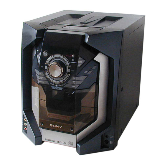
HCD-GSX100W is the Amplifier, CD player, Tape
Deck and Tuner section in MHC-GSX100W.
Main Unit
Amplifier section
For the U.S. model
AUDIO POWER SPECIFICATIONS
POWER OUTPUT AND TOTAL HARMONIC
DISTORTION:
With 6-ohm loads, both channels driven, from 120 – 10,000 Hz; rated 200
watts per channel minimum RMS power, with no more than 10% total
harmonic distortion from 250 milliwatts to rated output.
Continuous RMS power output (reference):
200 + 200 W(6 ohms at 1 kHz, 10%THD)
Total harmonic distortion less than 0.09% (6 ohms at 1 kHz, 125 W)
Inputs
VIDEO (MD) IN (phono jacks):
voltage 250/450 mV, impedance 47 kilohms
AUDIO IN (phono jacks): 450 mV, impedance 47 kilohms
Outputs
VIDEO OUT (phono jacks):
max. output level 1Vp-p, unbalanced, Sync
negative, load impedance 75 ohms
PHONES (stereo phone jack):
accepts headphones of 8 ohms or more
SPEAKER:
accepts impedance of 6 to 16 ohms
Sony Corporation
9-877-219-03
Home Audio Company
2003L02-1
Published by Sony Engineering Corporation
© 2003.12
HCD-GSX100W
CD
Section
TAPE
Section
SPECIFICATIONS
CD player section
System
Laser
Frequency response
Wavelength
Signal-to-noise ratio
Dynamic range
OPTICAL OUT (CD)
(Square optical connector jack, rear panel)
Wavelength
Output level
Tape deck section
Recording system
Frequency response
MiNi Hi-Fi COMPONENT SYSTEM
Canadian Model
Model Name Using Similar Mechanism
CD Mechanism Type
Base Unit Name
Optical Pick-up Name
Model Name Using Similar Mechanism
Tape Transport Mechanism Type
Compact disc and digital audio system
Semiconductor laser
(CD: λ=780 nm)
Emission duration: continuous
CD: 20 Hz – 20 kHz (±0.5 dB)
780 – 790 nm
More than 90 dB
More than 90 dB
660 nm
–18 dBm
4-track 2-channel stereo
40 – 13,000 Hz (±3dB),
using Sony TYPE I cassettes
US Model
HCD-GS300AV
CDM64C-K1BD47B
BU-K1BD47B
KSM-213BFN
HCD-GS300AV
CMAL1Z234A
— Continued on next page —
Advertisement
Table of Contents

Related Manuals for Sony HCD-GSX100W


Summary of Contents for Sony HCD-GSX100W
- Page 1 HCD-GSX100W SERVICE MANUAL US Model Canadian Model Ver 1.2 2003.12 HCD-GSX100W is the Amplifier, CD player, Tape Deck and Tuner section in MHC-GSX100W. Model Name Using Similar Mechanism HCD-GS300AV CD Mechanism Type CDM64C-K1BD47B Section Base Unit Name BU-K1BD47B Optical Pick-up Name...
-
Page 2: Table Of Contents
HCD-GSX100W Ver 1.1 2003.09 Tuner section General FM stereo, FM/AM superheterodyne tuner Power requirements: 120 V AC, 60 Hz FM tuner section Power consumption: 170 W Tuning range 87.5 – 108.0 MHz Dimensions (w/h/d) incl. projecting parts and controls Amplifier/Tuner/... -
Page 3: Leakage Test
CRITIQUES POUR LA SÉCURITÉ DE FONCTIONNEMENT. NE COMPONENTS WITH SONY PARTS WHOSE PART NUMBERS REMPLACER CES COMPOSANTS QUE PAR DES PIÈSES SONY APPEAR AS SHOWN IN THIS MANUAL OR IN SUPPLEMENTS DONT LES NUMÉROS SONT DONNÉS DANS CE MANUEL OU PUBLISHED BY SONY. -
Page 4: Servicing Notes
HCD-GSX100W SECTION 1 SERVICING NOTES CD-TEXT TEST DISC CLEANING OBJECTIVE LENS OF OPTICAL PICK-UP • In cleaning the objective lens of optical pick-up, be sure the following below. This unit is able to display the test data (character information) written in the CD on its fluorescent indicator tube. -
Page 5: General
HCD-GSX100W SECTION 2 GENERAL This section is extracted from instruction manual. MAIN UNIT BUTTON DESCRIPTIONS ALPHABETICAL ORDER I – Z A – H ?/1 (power) 1 ILLUMINATION 6 ALBM + qs Z PUSH (tape deck) 3 KEYBOARD INPUT jack ql ALBM –... - Page 6 HCD-GSX100W This section is extracted from instruction manual. REMOTE CONTROL BUTTON DESCRIPTIONS ALPHABETICAL ORDER A – Q R – Z ?/1 (power) 4 REPEAT 8 ALBM +/– qfwa nN (play) wf SLEEP 1 CD wl X (pause) wf SURROUND ql...
-
Page 7: Disassembly
HCD-GSX100W SECTION 3 Ver 1.1 2003.09 DISASSEMBLY • This set can be disassembled in the order shown below. TOP CABINET RX-BASE PC BOARD ASSY FRONT CABI ASSY MECH DECK (CMAL1Z234A), CASSETTE HOLDER BACK PANEL ASSY DETECT BOARD, MAIN BOARD AMP BOARD... -
Page 8: Top Cabinet
HCD-GSX100W Note: Follow the disassembly procedure in the numerical order given. 3-1. TOP CABINET 9 Three screws qf Top cabinet (BVTP3 × 10) 6 Two screws (BVTP3 × 10) 8 Panel side (L) 0 Connecter (CN101 ) 5 Three screws qa Wire (Flat type) (CN309 ) (BVTP3 ×... -
Page 9: Back Panel Assy
HCD-GSX100W 3-3. BACK PANEL ASSY 3 Two screws (BVTP 3x10) qs Back panel ASSY 7 Three screws (BVTP 3x10) 4 DC Fan (M351) 5 Two screws (BVTP 3x10) 1 Connector (CN356) 8 Four screws (BVTP 3x10) 9 Screw (BVTP 3x10) -
Page 10: Amp Board
HCD-GSX100W 3-5. AMP BOARD 2 Two screws (BVTP3 × 8) 4 Two screws (BVTP3 × 8) 3 Two screws (BVTP3 × 8) 1 Connector (CN353) 5 AMP board 3-6. POWER BOARD 2 Two screws (BVTP4 × 8) 1 Two screws (BVTP4 ×... -
Page 11: Holder (Led-S), Middle (R), Power Bracket
HCD-GSX100W Ver 1.1 2003.09 3-7. HOLDER (LED-S), MIDDLE (R) BRACKET, POWER BRACKET 5 Middle (R) bracket 4 Two screws (BVTP3 × 8) 3 Three screws 7 Two screws (BVTP3 × 8) (BVTP3 × 8) 8 Three screws 1 Two screws (BVTP3 ×... -
Page 12: Base Unit (Bu-K1Bd47B), D-Sensor (Out) Board, T-Sensor Board
HCD-GSX100W 3-9. BASE UNIT (BU-K1BD47B), D-SENSOR (OUT) BOARD, T-SENSOR BOARD 4 Screw (BVTP3 × 8) 5 D-SENSOR (OUT) board 3 Base unit (BU-K1BD47B) 2 Bracket (top 60) 1 Three screws (BVTP3 × 8) 6 Three screws (BVTP3 × 8) 7 T-SENSOR board 3-10. -
Page 13: Cd Led Board
HCD-GSX100W 3-11. CD LED BOARD Opens to right and left and CD LED BOARD 3 CD LED board is removed upwards from a slot. 3-12. BU HOLDER ASSY 1 Tension spring (F1) 2 Tension spring (F-2) 3 Two screws (PTP2.6 × 8) -
Page 14: Cd Board, Optical Pick-Up (Ksm-213Bfn)
HCD-GSX100W Ver 1.1 2003.09 3-13. CD BOARD, OPTICAL PICK-UP (KSM-213BFN) 7 Optical pick-up (KSM-213BFN) 5 Wire (Flat type) (CN102) 6 CD board 1 Remove two solders. 3 Screw (P2 × 5) 2 Remove two solders. 3-14. RX-BASE PC BOARD ASSY, MECHANICAL DECK (CMAL1Z234A), CASSETTE HOLDER... -
Page 15: Game Board, H/P Board
HCD-GSX100W 3-15. GAME BOARD, H/P BOARD Wire retainer pwb Harness Front cabinet 1 Two screws (BVTP2.6 × 8) 2 GAME board 3 Two screws (BVTP2.6 × 8) 4 Retainer H/P 5 H/P board 3-16. DISPLAY BOARD 4 Three screws (BVTP2.6 × 10) -
Page 16: Key (2) Board, Cd Sync Button
HCD-GSX100W 3-17. KEY (2) BOARD, CD SYNC BUTTON 1 Two screws (BVTP2.6 × 8) 3 Connector (CN706) 2 KEY (2) board 5 Two screws (BVTP3 × 10) 6 CD sync button 4 Screw(BVTP3 × 10) 3-18. KEY BOARD, WIRELESS BOARD 9 Four screws (BVTP3 ×... -
Page 17: Test Mode
HCD-GSX100W SECTION 4 TEST MODE [Panel Test Mode] [CD Service Mode] Procedure: • This mode can run the CD sled motor optionally. Use this mode, [MENU] [DISPLAY] 1. Press three buttons of , and simulta- for instance, when cleaning the optical pick-up. -
Page 18: Mechanical Adjustments
HCD-GSX100W SECTION 5 SECTION 6 MECHANICAL ADJUSTMENTS ELECTRICAL ADJUSTMENTS • TAPE MECHANISM DECK SECTION DECK SECTION 0 dB = 0.775 V Precaution 1. Clean the following parts with a denatured alcohol-moistened Precaution swab: 1. Demagnetize the record/playback head with a head demagne-... - Page 19 HCD-GSX100W Record/Playback Head Azimuth Adjustment Adjustment Location: Record/Playback/Erase Head Procedure: 1. Mode: Playback (FWD) test tape SPK board P-4-A100 SPEAKER terminal (J357) (10 kHz, – 10 dB) L-CH, R-CH Head azimuth level meter adjustment screw – 2. Turn the adjustment screw and check output peaks. If the peaks do not match for L-CH and R-CH, turn the adjustment screw so that outputs match within 1dB of peak.
- Page 20 HCD-GSX100W RFAC Level Check CD SECTION Connection: Note: oscilloscope 1. CD Block is basically designed to operate without adjustment. There- fore, check each item in order given. CD board 2. Use YEDS-18 disc (3-702-101-01) unless otherwise indicated. TP (RFAC) 3. Use an oscilloscope with more than 10MΩ impedance.
- Page 21 HCD-GSX100W E-F Balance Check Checking Location: Connection: – CD BOARD (Conductor Side) – oscilloscope CD board TP (TE1) TP (DVC) – Procedure: Connect an oscilloscpe to test point TP (TE1) and TP (DVC) on the CD board. Turn the power on.
-
Page 22: Circuit Boards Location
HCD-GSX100W SECTION 7 DIAGRAMS 7-1. Circuit Boards Location CD board AMP board RX unit D-SENSOR (OUT) board CD LED board TUNER board DISPLAY board DETCT board SPK board KEY board WIRELESS board POWER board MAIN board GAME board LOAD SW board... -
Page 23: Block Diagrams
HCD-GSX100W 7-2. Block Diagrams – CD Section – OPTICAL PICK-UP DIGITAL SERVO BLOCK DIGITAL SIGNAL PROSESSOR RF AMP (KSM-213BFN) IC101 IC103 IC309 OPTICAL OPTICAL RF AC RFAC D OUT OUT(CD) RFDCO RFDC D/A CONV, MP3 DECODER RFDCI IC104 L-OUT INPUT/EVR... -
Page 24: Tuner/Tape Deck Section
HCD-GSX100W – TUNER/TAPE DECK Section – TUNER PACK TUNER L-CH INPUT/EVR FM ANT L-CH SECTION FM 75Ω (Page 25) ANT GND R-CH R-CH • R-CH is omitted due to same as L-CH. AM ANT TU-DI • Signal Path ANT GND... -
Page 25: Input/Evr Section
HCD-GSX100W – INPUT/EVR Section – J301 REC-L TUNER/TAPE SECTION VIDEO IN (Page 24) (MD) R-CH INPUT SELECT SWITCH, J701 GRAPHIC EQUALIZER CONTROL, R-CH GAME-L ELECTRICAL VOLUME IC301 J304 AUDIO SWOUT GAME R-CH VIDEO OUT INPUT VIDEO MID/ VOLIN1 TOUT1 FRONT... -
Page 26: Amp Section
HCD-GSX100W – AMP Section – J882 PHONES DBFB INPUT/EVR SECTION POWER AMP (Page 25) J357 IC601 FRONT INPUT/EVR L-CH IN/CH1 +RE/CH2 SECTION -RE/CH2 (Page 25) – +RE/CH1 SPEAKER R-CH IN/CH2 -RE/CH1 – -PRE RY501 OVER LOAD MUTING DETECT Q517, 518... -
Page 27: Display/Power Supply Section
HCD-GSX100W – DISPLAY/POWER Supply Section – DISPLAY CONTROLLER IC701 KEY 1 FUNCTION KEY S751 – 756 FL701 FLUORESCENT KEY 0 FUNCTION KEY INDICATOR TUBE S770 – 777 VP-30V GRID DRIVE Q723 - 726 KEY 2 FUNCTION KEY VF1,2 S760 – 769... -
Page 28: Printed Wiring Board - Cd Section
HCD-GSX100W Ver 1.1 2003.09 7-3. Printed Wiring Board – CD Section – • See page 22 for Circuit Boards Location. D202 D201 x C262 C208 R293 x C261 C293 (12) (12) • Semiconductor Location Ref. No. Location D201 D202 IC101... -
Page 29: Schematic Diagram - Cd Section
HCD-GSX100W Ver 1.1 2003.09 7-4. Schematic Diagram – CD Section – • See page 48 for IC Pin Function Description. -
Page 30: Cd Motor/Sensor Section
HCD-GSX100W 7-5. Printed Wiring Board – CD MOTOR/SENSOR Section – • See page 22 for Circuit Boards Location. L.T MOTOR BOARD T–SENSOR BOARD MAIN BOARD M441 (Page 32) LOADING MOTOR M442 TABLE MOTOR 1-687-592- (11) MAIN BOARD (Page 32) 1-687-589- (11) D–SENSOR(OUT) BOARD... -
Page 31: Cd Motor/Sensor Section
HCD-GSX100W 7-6. Schematic Diagram – CD MOTOR/SENSOR Section – (Page 33) (Page 33) (Page 33) (Page 33) (Page 33) -
Page 32: Printed Wiring Board - Main Section
HCD-GSX100W 7-7. Printed Wiring Board – MAIN Section – • See page 22 for Circuit Boards Location. DETECT BOARD BOARD (Page 44) TAPE TAPE (Page 38) MECHANISM MECHANISM BOARD DECK DECK TUNER PACK (Page 36) BLOCK BLOCK (REC-PB/ERASE HEAD) (CAPSTAN MOTOR/PLUNGER) -
Page 33: Schematic Diagram - Main Section (1/3)
HCD-GSX100W 7-8. Schematic Diagram – MAIN Section (1/3) – R118... -
Page 34: Schematic Diagram - Main Section (2/3)
HCD-GSX100W 7-9. Schematic Diagram – MAIN Section (2/3) – • See page 50 for IC Pin Function Description. -
Page 35: Schematic Diagram - Main Section (3/3)
HCD-GSX100W 7-10. Schematic Diagram – MAIN Section (3/3) –... -
Page 36: Printed Wiring Board - Amp Section
HCD-GSX100W 7-11. Printed Wiring Board – AMP Section – • See page 22 for Circuit Boards Location. SPK BOARD SPEAKER MAIN BOARD M351 (Page 32) H/P JACK BOARD DC FAN 1-687-599- (11) AMP BOARD 1-687-603- (11) PHONES POWER BOARD (Page 42) •... -
Page 37: Schematic Diagram - Amp Section
HCD-GSX100W 7-12. Schematic Diagram – AMP Section –... -
Page 38: Printed Wiring Board - Display Section
HCD-GSX100W 7-13. Printed Wiring Board – DISPLAY Section – • See page 22 for Circuit Boards Location. MAIN MAIN BOARD BOARD BOARD BOARD (Page 40) (Page 32) (Page 40) (Page 32) CD LED BOARD DISPLAY BOARD 1-687-593- (11) GAME GAME BOARD... -
Page 39: Schematic Diagram - Display Section
HCD-GSX100W 7-14. Schematic Diagram – DISPLAY Section – • See page 52 for IC Pin Function Description. -
Page 40: Printed Wiring Board - Key Section
HCD-GSX100W 7-15. Printed Wiring Board – KEY Section – • See page 22 for Circuit Boards Location. KEY BOARD PAUSE/START DISPLAY MENU ENTER ILLUMINATION PLAY MODE/ DIRECTION FM MODE REPEAT CLEAR ALBM – ALBM + DISC SELECT MAIN A GND B... -
Page 41: Schematic Diagram - Key Section
HCD-GSX100W 7-16. Schematic Diagram – KEY Section –... -
Page 42: Printed Wiring Board - Power Section
HCD-GSX100W 7-17. Printed Wiring Board – POWER Section – • See page 22 for Circuit Boards Location. POWER BOARD T901 POWER TRANSFORMER * NOT REPLACEABLE: BUILT IN TRANSFORMER MAIN BOARD (Page 32) 1-687-602- (11) BOARD AC IN (Page 36) -
Page 43: Schematic Diagram - Power Section
HCD-GSX100W 7-18. Schematic Diagram – POWER Section –... -
Page 44: Printed Wiring Board - Rx Section
HCD-GSX100W 7-19. Printed Wiring Board – RX Section – • See page 22 for Circuit Boards Location. MAIN BOARD RX BOARD (SIDE A) (Page 32) RX BOARD (SIDE B) FRONT END BLOCK FE80 1-687-587- 1-687-587- (11) (11) Note : RX board can´t be repair. -
Page 45: Schematic Diagram - Rx Section
HCD-GSX100W 7-20. Schematic Diagram – RX Section – Note : RX board can´t be repair. In case of a repair, exchange to RX BOARD ASSY. -
Page 46: Ic Block Diagrams
HCD-GSX100W 7-21. IC Block Diagrams • Waveforms – CD Board – – MAIN Board – – DISPLAY Board – – CD Board – IC101 t; (RFAC) IC801 qd (XOUT) IC701 id (X1) (CD Play Mode) IC103 CXA2581N-T4 RW/ROM 3.8Vp-p 0.96Vp-p 1.7Vp-p... - Page 47 HCD-GSX100W – MAIN Board – IC101 CXD3068Q IC401 BA6780 VIN1 VIN2 FIN1 FIN2 RIN1 RIN2 IOUT VREF VREG FBIN- FBIN+ OUT2+ OUT1+ OUT2-...
-
Page 48: Ic Pin Function Description
HCD-GSX100W 7-22. IC Pin Function Description • IC104 TC94A20F-CX4 D/A Converter, MP3 Decoder (CD Board) Pin No. Pin Name Description RESET Reset input terminal “L”: reset MIMD Microcomputer interface mode selection input “H”: I2C, “L”: TSB MICS/AD0 Microcomputer interface chip select signal input... - Page 49 HCD-GSX100W Pin No. Pin Name Description VSSP – Ground for VCO circuit PLL phase error detection signal output VCOI VCO control voltage input VDDP – Power supply (2.5V) for VCO circuit External clock output VDDX – Power supply (2.5V) for oscillation circuit...
- Page 50 HCD-GSX100W • IC801 M30624MGN-A16FP System Controller (MAIN Board) Pin No. Pin Name Description TABLE POS Table motor control signal output to the motor driver (IC401) LOAD POS Loading motor control signal output to the motor driver (IC401) LOAD NEG Loading motor control signal output to the motor driver (IC401)
- Page 51 HCD-GSX100W Pin No. Pin Name Description PL-DATA Serial data output to the PROLOGIC IC (Not used) PL-CLK Serial clock ouput to the PROLOGIC IC (Not used) PL-RQ Request signal output to the PROLOGIC IC (Not used) VOL-CLK Clock output to the VOLUME IC (IC301)
- Page 52 HCD-GSX100W • IC701 MB90M407APF-G-126-BND Display Controller (DISPLAY Board) Pin No. Pin Name Description LED16/PIP16 Grid drive signal output to the fluorescent indicator tube (FL701) 2 to 6 FIP17 to FIP21 Grid drive signal output to the fluorescent indicator tube (FL701)
-
Page 53: Exploded Views
HCD-GSX100W SECTION 8 Ver 1.1 2003.09 EXPLODED VIEWS NOTE: • -XX, -X mean standardized parts, so they may • The mechanical parts with no reference number The components identified by mark 0 or have some differences from the original one. -
Page 54: Front Panel Section
HCD-GSX100W 8-2. FRONT PANEL SECTION supplied FL701 supplied supplied supplied supplied supplied SW701 supplied with RV752 supplied not supplied Ref. No. Part No. Description Remark Ref. No. Part No. Description Remark 4-244-590-11 LID,CD(FRONT) 4-244-726-01 INDICATOR WIRELESS 4-244-589-01 KNOB,DISC 4-244-588-01 KNOB,VOLUME... -
Page 55: Chassis Section
HCD-GSX100W Ver 1.2 8-3. CHASSIS SECTION Mechanism Deck section (CDM64C-K1BD47B) F902 supplied supplied T901 supplied not supplied Ref. No. Part No. Description Remark Ref. No. Part No. Description Remark 0 F902 4-231-311-02 TABLE (60) 1-533-454-11 FUSE, GLASS TUBE (DIA. 5) (6.3A 125V) -
Page 56: Mechanism Deck Section-1 (Cdm64C-K1Bd47B)
HCD-GSX100W Ver 1.1 2003.09 8-4. MECHANISM DECK SECTION-1 (CDM64C-K1BD47B) not supplied not supplied Base Unit Section (BU-K1BD47B) not supplied not supplied not supplied Ref. No. Part No. Description Remark Ref. No. Part No. Description Remark * 502 4-976-474-01 HOLDER (P-T) -
Page 57: Mechanism Deck Section-2 (Cdm64C-K1Bd47B)
HCD-GSX100W Ver 1.1 2003.09 8-5. MECHANISM DECK SECTION-2 (CDM64C-K1BD47B) not supplied M441 M442 not supplied Ref. No. Part No. Description Remark Ref. No. Part No. Description Remark 4-216-067-01 SPRING (CLAMP), COMPRESSION 4-216-078-01 LEVER (LOADING) 3-701-441-21 WASHER A-4672-676-B CAM ASSY X-4954-587-1 HOLDER (DISC-L) ASSY 4-933-134-21 SCREW (+PTPWH M2.6X10) -
Page 58: Base Unit Section (Bu-K1Bd47B)
HCD-GSX100W Ver 1.1 2003.09 8-6. BASE UNIT SECTION (BU-K1BD47B) Ref. No. Part No. Description Remark Ref. No. Part No. Description Remark A-4734-813-A CD BOARD COMPLETE 1-824-104-11 WIRE (FLAT TYPE) (29 CORE) 0 602 A-3328-818-A DEVICE,OPTICAL (KSM-213BFN) 4-992-054-11 RUBBER, VIBRATION PROOF... -
Page 59: Electrical Parts List
HCD-GSX100W SECTION 9 ELECTRICAL PARTS LIST Ref. No. Part No. Description Remarks Ref. No. Part No. Description Remarks NOTE: When indicating parts by reference number, • Due to standardization, replacements in the • COILS please include the board name. parts list may be different from the parts uH: µH... - Page 60 HCD-GSX100W Ref. No. Part No. Description Remarks Ref. No. Part No. Description Remarks < JUNPER RESISTOR > R251 1-216-820-11 METAL CHIP 1/10W R252 1-216-820-11 METAL CHIP 1/10W JR150 1-216-864-11 METAL CHIP 1/10W R253 1-216-841-11 METAL CHIP 1/10W JR151 1-216-864-11 METAL CHIP...
- Page 61 HCD-GSX100W Ver 1.1 2003.09 Ref. No. Part No. Description Remarks Ref. No. Part No. Description Remarks A-4734-813-A CD BOARD, COMPLETE C261 1-126-916-11 ELECT 1000uF 6.3V C262 1-126-916-11 ELECT 1000uF 6.3V ****************** < CAPACITOR > C263 1-125-822-11 TANTAL. CHIP 10uF C264...
- Page 62 HCD-GSX100W Ver 1.1 2003.09 DETECT CD LED D-SENSOR (IN) D-SENSOR (OUT) Ref. No. Part No. Description Remarks Ref. No. Part No. Description Remarks R120 1-216-846-11 METAL CHIP 120K 1/10W CD LED BOARD R122 1-216-845-11 METAL CHIP 100K 1/10W ************* R123...
- Page 63 HCD-GSX100W DETECT DISPLAY GAME Ref. No. Part No. Description Remarks Ref. No. Part No. Description Remarks R606 1-216-851-11 METAL CHIP 330K 1/10W JR716 1-216-864-11 METAL CHIP 1/10W R607 1-216-833-11 METAL CHIP 1/10W JR717 1-216-864-11 METAL CHIP 1/10W R608 1-216-833-11 METAL CHIP...
- Page 64 HCD-GSX100W Ref. No. Part No. Description Remarks Ref. No. Part No. Description Remarks H/P BOARD R763 1-216-819-11 METAL CHIP 1/10W R764 1-216-821-11 METAL CHIP 1/10W ********** R765 1-216-823-11 METAL CHIP 1.5K 1/10W < CAPACITOR > R766 1-216-825-11 METAL CHIP 2.2K...
- Page 65 HCD-GSX100W KEY(2) LOAD SW MAIN Ref. No. Part No. Description Remarks Ref. No. Part No. Description Remarks KEY (2) BOARD C211 1-130-470-00 MYLAR 820PF C212 1-126-964-11 ELECT 10uF ************* < CONNECTOR > C213 1-136-165-00 FILM 0.1uF C214 1-136-165-00 FILM 0.1uF...
- Page 66 HCD-GSX100W MAIN Ref. No. Part No. Description Remarks Ref. No. Part No. Description Remarks C466 1-126-964-11 ELECT 10uF < CONNECTOR > C467 1-126-960-11 ELECT * CN301 1-564-511-11 PLUG, CONNECTOR 8P C468 1-126-964-11 ELECT 10uF CN305 1-779-297-11 CONNECTOR,FFC(LIF(NON-ZIF))29P C469 1-162-964-11 CERAMIC CHIP 0.001uF...
- Page 67 HCD-GSX100W MAIN Ref. No. Part No. Description Remarks Ref. No. Part No. Description Remarks IC801 6-802-612-01 IC M30624MGN-A16FP Q931 8-729-019-00 TRANSISTOR 2SD2394-G IC802 8-759-533-04 IC M62703ML-E1 Q934 8-729-037-13 TRANSISTOR KTA1271Y IC803 6-701-760-01 IC uPC3504AHF < RESISTOR > IC931 8-759-646-52 IC KIA7805API...
- Page 68 HCD-GSX100W MAIN Ref. No. Part No. Description Remarks Ref. No. Part No. Description Remarks R318 1-216-821-11 METAL CHIP 1/10W R468 1-216-833-11 METAL CHIP 1/10W R319 1-216-821-11 METAL CHIP 1/10W R469 1-218-867-11 METAL CHIP 6.8K 1/10W R320 1-216-821-11 METAL CHIP 1/10W...
- Page 69 HCD-GSX100W MAIN POWER SPK T-SENSOR Ref. No. Part No. Description Remarks Ref. No. Part No. Description Remarks R824 1-216-815-11 METAL CHIP 1/10W D902 8-719-063-79 DIODE 1N4002B D903 8-719-063-79 DIODE 1N4002B R825 1-216-821-11 METAL CHIP 1/10W D904 8-719-063-79 DIODE 1N4002B R826 1-216-829-11 METAL CHIP 4.7K...
- Page 70 HCD-GSX100W Ver 1.1 2003.09 WIRELESS Ref. No. Part No. Description Remarks WIRELESS BOARD **************** < DIODE > D740 6-500-620-01 DIODE SLR343BBT3FXG D741 6-500-620-01 DIODE SLR343BBT3FXG < RESISTOR > R777 1-216-809-11 METAL CHIP 1/10W R778 1-216-809-11 METAL CHIP 1/10W ************************************************************* MISCELLANEOUS...
- Page 71 HCD-GSX100W MEMO Ref. No. Part No. Description Remarks Ref. No. Part No. Description Remarks...
- Page 72 HCD-GSX100W REVISION HISTORY Clicking the version allows you to jump to the revised page. Also, clicking the version at the upper right on the revised page allows you to jump to the next revised page. Ver. Date Description of Revision 2003.03...