Table of Contents
Advertisement
Quick Links
QQ
3 7 63 1515 0
SERVICE MANUAL
Ver 1.1 2003. 09
HCD-M700 is the Amplifier, DVD player,
MD deck, Tape player and Tuner section in
CMT-M700MD.
TE
L 13942296513
Amplifier section
European model:
DIN power output (rated): 15 + 15 W
Continuous RMS power output (reference):
Music power output (reference):
Other models:
The following measured at 230 V AC, 60 Hz
DIN power output (rated): 15 + 15 W
Continuous RMS power output (reference):
The following measured at 220 V AC, 60 Hz
DIN power output (rated): 12 + 12 W
Continuous RMS power output (reference):
www
.
Sony Corporation
9-874-037-02
Home Audio Company
2003I16-1
Published by Sony Engineering Corporation
© 2003.09
http://www.xiaoyu163.com
Inputs
ANALOG IN:
(phono jacks)
(6 ohms at 1 kHz, DIN)
DIGITAL OPTICAL IN (supported sampling
frequencies: 32 kHz, 44.1 kHz and 48 kHz)
20 + 20 W
Outputs
(6 ohms at 1 kHz, 10%
VIDEO OUT:
THD)
(phono jack)
40 + 40 W
S-VIDEO OUT:
(4-pin/mini-DIN jack)
(6 ohms at 1 kHz, DIN)
DIGITAL OPTICAL OUT: Optical
18 + 18 W
PHONES:
(6 ohms at 1 kHz, 10%
THD)
SPEAKER:
(6 ohms at 1 kHz, DIN)
15 + 15 W
(6 ohms at 1 kHz, 10%
THD)
x
ao
u163
y
i
http://www.xiaoyu163.com
HCD-M700
2 9
8
Model Name Using Similar Mechanism
CD Mechanism Type
DVD
Base Unit Type
Section
Optical Pick-up Type
Q Q
Model Name Using Similar Mechanism
3
6 7
1 3
1 5
MD
MD Mechanism Type
Section
Optical Pick-up Type
Tape deck
Model Name Using Similar Mechanism
Section
Tape Transport Mechanism Type
SPECIFICATIONS
Sensitivity 250 mV,
impedance 47 kilohms
max. output level
1 Vp-p, unbalanced, Sync
negative, load impedance
75 ohms
Y: 1 Vp-p, unbalanced,
Sync negative,
C: 0.286Vp-p,
load impedance 75 ohms
Wavelength: 660 nm
Accepts headphones with
an impedance of 8 ohms
or more
accepts impedance of 6 to
16 ohms.
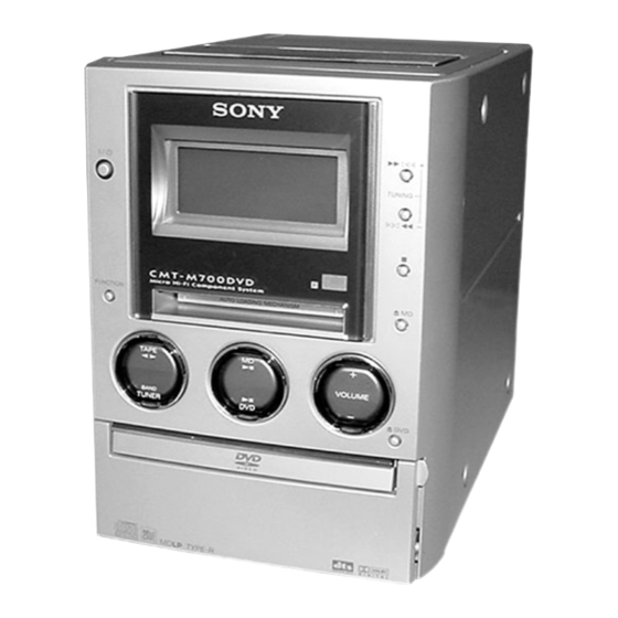
MICRO HI-FI COMPONENT SYSTEM
co
.
9 4
2 8
AEP Model
UK Model
E Model
NEW
CDM55A-DVBU8
DVBU8
KHM-240AAA (TYPE A)
KHM-270AAA (TYPE B)
HCD-M10
0 5
8
2 9
9 4
2 8
MDM-7B4M
KMS-260B
NEW
CMAL1Z228
DVD player section
Laser
Semiconductor laser
(DVD: λ=650 nm,
CD: λ=780 nm)
Emission duration:
continuous
Frequency response
DVD (PCM 48 kHz):
2 Hz – 22 kHz
CD: 2 Hz – 20 kHz
Video color system format
NTSC, PAL
MD deck section
System
Minidisc digital audio
system
Laser
Semiconductor laser
(λ=780 nm)
Emission duration:
continuous
Sampling frequency
44.1 kHz
Frequency response
5 Hz – 20 kHz
— Continued on next page —
m
9 9
9 9
Advertisement
Table of Contents

Related Manuals for Sony hcd-m700


Summary of Contents for Sony hcd-m700
- Page 1 3 7 63 1515 0 SERVICE MANUAL AEP Model UK Model Ver 1.1 2003. 09 E Model HCD-M700 is the Amplifier, DVD player, MD deck, Tape player and Tuner section in CMT-M700MD. Model Name Using Similar Mechanism CD Mechanism Type CDM55A-DVBU8...
- Page 2 COMPONENTS IDENTIFIED BY MARK 0 OR DOTTED LINE WITH MARK 0 ON THE SCHEMATIC DIAGRAMS AND IN THE PARTS LIST ARE CRITICAL TO SAFE OPERATION. REPLACE THESE COMPONENTS WITH SONY PARTS WHOSE PART NUMBERS APPEAR AS SHOWN IN THIS MANUAL OR IN SUPPLEMENTS PUBLISHED BY SONY.
-
Page 3: Table Of Contents
HCD-M700 Ver 1.1 2003.09 3 7 63 1515 0 TABLE OF CONTENTS 6-10. Schematic Diagram – DVD Board (2/8) – ························ 67 1. SERVICING NOTES ···················································· 10 6-11. Schematic Diagram – DVD Board (3/8) – ························ 68 6-12. Schematic Diagram – DVD Board (4/8) – ························ 69 2. - Page 4 No component is connected to the DIGITAL the problem refer to the following list. If any OPTICAL IN jack, or you tried to record from the problem persists, consult your nearest Sony digital component which is not connected dealer. correctly.
- Page 5 Cannot REC cContact your nearest Sony dealer or local • A pre-mastered MD is in the deck. authorized Sony service facility and give the 5- L 13942296513 • The function is switched to MD. character service number.
- Page 6 HCD-M700 3 7 63 1515 0 Self-diagnosis display (continued) TOC Writing The MD deck is writing the information of recorded or edited contents. Incomplete! Track End Adjustment of the recording level after recording You have reached the end of the track while...
- Page 7 HCD-M700 3 7 63 1515 0 Note 1: About “R” As this unit has only a few buttons, some operations require the use of remote commander (RM-SM700E/provided with unit) buttons. These operations are indicated as “R” in this manual.
- Page 8 HCD-M700 3 7 63 1515 0 Items of Error History Mode Items and Contents Selecting the Test Mode Display History op rec tm Displays the accumulated recording time. When the accumulated recording time is more than 1 minute, displays the hour and minute When less than 1 minute, displays “Under 1 min”...
- Page 9 HCD-M700 3 7 63 1515 0 Table of Error Codes Error Code Description Could not perform loading The changer error occurred Loading switches combined incorrectly Timed out without reading the top of PTOC Could read top of PTOC, but detected error...
-
Page 10: Servicing Notes
HCD-M700 SECTION 1 SERVICING NOTE 3 7 63 1515 0 Jig For Checking BD Board Waveform The special jig (J-2501-196-A) is useful for checking the waveform of the BD board. The names of terminals and the checking items to be performed are shown as follows. - Page 11 HCD-M700 3 7 63 1515 0 Jig For Checking DVD Board and DIGITAL Board Waveform The special jig (J-2501-196-A) is useful for checking the waveform of the DVD board and DIGITAL board. • Extention cable (10P) (J-2501-219-A) • Extention cable (27P)
- Page 12 HCD-M700 3 7 63 1515 0 Iop DATA RECORDING AND DISPLAY WHEN OPTICAL PICK-UP AND NON-VOLATILE MEMORY (IC195 OF BD BOARD) ARE REPLACED The Iop value labeled on the optical pick-up can be stored in the non-volatile memory. By storing the value, it will eliminate the need to look at the value on the label of the optical pick-up.
-
Page 13: General
HCD-M700 SECTION 2 This section is extracted GENERAL 3 7 63 1515 0 from instruction manual. Main unit BUTTON DESCRIPTIONS ALPHABETICAL ORDER ?/1 (power) 1 A – P R – V m/M 3 DIRECTION qk (63–65) REC MODE qg (40–42) -
Page 14: Remote Control
HCD-M700 3 7 63 1515 0 Remote Control ALPHABETICAL ORDER P – V A – D E – N ANGLE eg (28) ENTER/YES wd (11, 14, 35, PLAY MODE/TUNING MODE 0 (12, 14, 15, 33, 35, 41, 47, 42–60, 62, 68–70) AUDIO ej (25) 60–62) - Page 15 HCD-M700 3 7 63 1515 0 Setting the clock Press ?/1 to turn on the system. Press CLOCK/TIMER SET on the remote. Press MENU + or – on the remote repeatedly to set the hour. Press ENTER/YES or CURSORt on the remote.
-
Page 16: Disassembly
HCD-M700 Ver 1.1 2003.09 SECTION 3 DISASSEMBLY 3 7 63 1515 0 • The equipment can be removed using the following procedure. TC BOARD, CASE (R), CASE (L), SET (HCD-M700E) MECHANISM DECK TOP COVER SECTION (CMAL1Z228) FRONT PANEL SECTION,... -
Page 17: Case (R), Case (L), Top Cover Section
HCD-M700 3 7 63 1515 0 Note: Follow the disassembly procedure in the numerical order given. 3-1. Case (R), Case (L), Top Cover Section 7 screw (+BVTP 3 × 10) top cover section 8 case (L) 6 two screws (3 ×... -
Page 18: Video Board, Optical Board
HCD-M700 3 7 63 1515 0 3-3. VIDEO Board, OPTICAL Board three screws (+BVTP 3 × 10) 5 VIDEO board three screws (+BVTP 3 × 10) 6 OPTICAL board back panel 4 RETEINER board 3 screw (+BVTP 3 × 8 ) L 13942296513 3-4. -
Page 19: Tc Board, Mechanism Deck (Cmal1Z228)
HCD-M700 3 7 63 1515 0 3-5. TC Board, Mechanism Deck (CMAL1Z228) top cover 8 cover 7 mechanism deck (CMAL1Z228) hook four screws (+BVTP 3 × 8 ) 3 Remove the cut-out portion of TC board from the hook of mechanism deck n the direction of the arrow. -
Page 20: Control Board
HCD-M700 3 7 63 1515 0 3-7. CONTROL Board 3 two screws (+BVTP 3 × 8 ) 1 flexible flat cable (CN608) CONTROL board 2 flexible flat cable (CN607) L 13942296513 3-8. POWER Board 3 four screws (+BVTP 4 × 6 ) -
Page 21: Digital Board
HCD-M700 3 7 63 1515 0 3-9. DIGITAL Board 2 four screws (+BVTP 3 × 8 ) 1 flexible flat cable (CN705) 3 cover (MD)2 5 flexible flat cable (CN701) 4 flexible flat cable (CN702) 8 DIGITAL board 6 flexible flat cable... -
Page 22: Dvd Board
HCD-M700 3 7 63 1515 0 3-11. DVD Board 1 connector (CN008) POWER board) screw (+BVTP 3 × 8 ) MD bracket two screws (+BVTP 3 × 8 ) four screws (+BVTP 3 × 8 ) DVD board 6 connector... -
Page 23: Holder Assy
HCD-M700 3 7 63 1515 0 3-13. Holder Assy 5 holder assy 1 tension spring (holder) 2 hook L 13942296513 3-14. BD Board Remove soldering from the two points. (sled) Remove soldering from the two points. (spindle) M102 flexible flat cable... -
Page 24: Over Light Head (Hr901)
HCD-M700 3 7 63 1515 0 3-15. Over Light Head (HR901) 1 screw (P 1.7 × 6 ) 2 over light head (HR901) 3-16. OP-SUB Assy L 13942296513 9 OP-SUB assy 6 main shaft 3 screw (+BP TRI 2 × 6 CZN ) -
Page 25: Loading Motor Assy (M103), Spinde Motor Assy (M101)
HCD-M700 3 7 63 1515 0 3-17. Loading Motor Assy (M103), Spinde Motor Assy (M101), Sled Motor Assy (M102) 3 torsion spring (SPDL) 1 lever (HEAD) 2 belt (loading) 8 two screws (+PWH 1.7x 3.5) 4 two screws (+PWH 1.7x 3.5) -
Page 26: Board
HCD-M700 3 7 63 1515 0 3-19. RF-240 Board 4 RF-240 board 2 flexible flat cable (CN001) 1 flexible flat cable (CN002) 3 three screws (+BTP 2.6 × 6) L 13942296513 3-20. Tray 1 While pressing the two protrusions A and B to unlock the two claws as shown, pull the tray in the direction of the arrow C . -
Page 27: Optical Pick Up (Khm-240Aaa(Type A))
HCD-M700 Ver 1.1 2003.09 3 7 63 1515 0 3-21. Optical Pick Up (KHM-240AAA(TYPE A))(KHM-270AAA(TYPE B)) 3 chassis section three insurators 5 two step screws (M) 4 step screw (L) 6 flexible flat cable (9core) 8 holder (KHM-240) optical pick up (KHM-240AAA(TYPE A) -
Page 28: Test Mode
HCD-M700 SECTION 4 TEST MODE 3 7 63 1515 0 Note 1: About “R” As this unit has only a few buttons, some operations require the use of remote commander (RM-SM700E/provided with unit) buttons. These operations are indicated as “R” in this manual. - Page 29 HCD-M700 3 7 63 1515 0 DVD Ship Mode (Setting the Position for Transportation) Press ?/1 button to turn the power on. Press FUNCTION to change the function to “DVD”. Press three buttons x , ENTER/START and DVD u simultaneously.
- Page 30 HCD-M700 3 7 63 1515 0 5. Selecting the Test Mode There are 26 types of test modes as shown below. The groups can be switched by pressing the MD “R” or MD “R” button. > After selecting the group to be used, press the ENTER/YES “R” button. After setting a certain group, pressing the MD “R”...
- Page 31 HCD-M700 3 7 63 1515 0 5-1. Operating the Continuous Playback Mode Entering the continuous playback mode (1) Set the disc in the unit. (Whichever recordable discs or discs for playback only are available) (2) Press the MD “R” or MD “R”...
- Page 32 HCD-M700 3 7 63 1515 0 7. Automatic Self-diagnosis Function This test mode performs CREC and CPLAY automatically for mainly checking the characteristics of the optical pick-up. To perform this test mode, the laser power must first be checked.
-
Page 33: Electrical Adjustments
HCD-M700 SECTION 5 ELECTRICAL ADJUSTMENTS 3 7 63 1515 0 MD SECTION Note 1: About “R” As this unit has only a few buttons, some operations require the use of remote commander (RM-SM700E/provided with unit) buttons. These operations are indicated as “R” in this manual. - Page 34 HCD-M700 3 7 63 1515 0 Flow Chart for Adjustment Start After turning the power off and on, initialises the non-volatile IC195 replacement memory (EEPROM). 7. Initial setting of adjustment value (See page 39) OP or IC195 replacement IC101, IC195 or D101 9.
- Page 35 HCD-M700 3 7 63 1515 0 Precautions for Checking Laser Diode 5. When observing several signals on the oscilloscope, etc., make sure that VC and ground do not connect inside the Emission oscilloscope. To check the emission of the laser diode during adjustments, never (VC and ground will become short-circuited.)
- Page 36 HCD-M700 3 7 63 1515 0 Using the Continuously Recorded Disc Procedure: 1. Set the laser power meter on the objective lens of the optical * This disc is used in focus bias adjustment and error rate check. pick-up. (When it cannot be set properly, press the m button The following describes how to create a continuous recording or M button to move the optical pick-up.)
- Page 37 HCD-M700 3 7 63 1515 0 6-4. Auto Check 6-6. Traverse Check This test mode performs CREC and CPLAY automatically for mainly checking the characteristics of the optical pick-up. To Note 1: Data will be erased during MO reading if a recorded disc is used in this adjustment.
- Page 38 HCD-M700 3 7 63 1515 0 6-7. Focus Bias Check 9. Press the ENTER/YES “R” button to display “EFB = Change the focus bias and check the focus tolerance amount. MO-P”. Procedure: Then, the optical pick-up moves to the pit area automatically 1.
- Page 39 HCD-M700 3 7 63 1515 0 Initial Setting of Adjustment Value Procedure: 1. Press the MD “R” or MD > “R” button to display “TEMP ADJUST” (C03). Note: Mode which sets the adjustment results recorded in the non-volatile 2. Press the ENTER/YES “R” button to select the “TEMP memory to the initial setting value.
- Page 40 HCD-M700 3 7 63 1515 0 6. Press the MD “R” or MD “R” button so that the 11. Iop NV Save > reading of the laser power meter becomes the specified value, Write the reference values in the nonvolatile memory to perform press the ENTER/YES “R”...
- Page 41 HCD-M700 3 7 63 1515 0 8. Press the MD “R” or MD “R” button so that the > 18. Press the ENTER/YES “R” button, display “EFB = SAVE” waveform of the oscilloscope becomes the specified value. for a moment and save the adjustment results in the non-volatile (When the MD “R”...
- Page 42 HCD-M700 3 7 63 1515 0 14. Error Rate Check 16. Auto Gain Control Output Level Adjustment Be sure to perform this adjustment when the optical pick-up is 14-1. CD Error Rate Check replaced. Procedure: If the adjustment results becomes “Adjust NG!”, the optical pick- 1.
- Page 43 HCD-M700 3 7 63 1515 0 Adjustment and checking Loacation: – BD BOARD (Side A) – – BD BOARD (Side B) – CN101 D101 IC101 CN105 IC102 IC151 IC190 IC195 CN103 CN102 Note: It is useful to use the jig for checking the waveform. (Refer to Ser-...
- Page 44 HCD-M700 3 7 63 1515 0 Syscon Diagnosis DVD SECTION The same contents as board detail check by serial interface can be checked from the remote commander. Note 1: About “R” As this unit has only a few buttons, some operations require On the Test Mode Menu screen, press the 0 “R”...
- Page 45 HCD-M700 3 7 63 1515 0 Press the DVD x “R” button to end the diagnosis. Press the (4-3) DSP Driver Test Test signal data → DSP driver DVD . “R” button to re-check the error ocurrence point. Press the DVD >...
- Page 46 HCD-M700 3 7 63 1515 0 (5-4) ARP to RAM Address Bus (6-3) 1930 SP Data write → other address read discord check ROM → AVD RAM → Video OUT Error 10: ARP ↔ RAM address bus error Error: Not detected.
- Page 47 HCD-M700 3 7 63 1515 0 Error Codes List 1. DVD-SL (single layer) 00: Error not detected Press the 1 key on the remote commander, insert DVD single layer 01: RAM write/read data discord disc, and press ENTER “R” key on the remote commander, and...
- Page 48 HCD-M700 3 7 63 1515 0 2. CD 3. DVD-DL (dual layer) Press the 2 key on the remote commander, insert CD disc, and Press the 3 key on the remote commander, insert DVD dual layer press ENTER “R” key on the remote commander, and the disc, and press ENTER “R”...
- Page 49 HCD-M700 3 7 63 1515 0 4. SACD (SACD hybrid disc) Drive Manual Operation Press the 4 key on the remote commander, insert a SACD hybrid On the Test Mode Menu screen, Press the 2 key on the remote disc, and press the ENTER “R”...
- Page 50 HCD-M700 3 7 63 1515 0 0. Disc Check Memory Disc Type 1. Disc Type Auto Check Disc Check 2. DVD SL 12 cm 3. DVD DL 12 cm 4. CD 12cm 5. LCD 12 cm 1. SL Disc Check 6.
- Page 51 HCD-M700 3 7 63 1515 0 The following menus are normally not used. Mechanism Aging 3. Track/Layer Jump ### Mecha Aging ### 4. Manual Adjustment Press OPEN Key 5. Auto Adjustment The persons who do not know well about these menus should not use them.
- Page 52 HCD-M700 3 7 63 1515 0 Emergency code table (1) Video level adjustment (DVD board) <Purpose> 10. Communication error with IC001 (RF-240 board) To align the video output signal level with the NTSC standard. If 11. Servo lock of focus, tracking and spindle servos are lost.
- Page 53 HCD-M700 3 7 63 1515 0 Adjustment Related Components Location Diagram DVD board (side A) CN402 CN010 CN009 IC103 IC503 RV501 VIDEO LEVEL Adjustment L 13942296513 CN008 CN404 CN103 CN101 u163 http://www.xiaoyu163.com...
-
Page 54: Diagrams
HCD-M700 SECTION 6 DIAGRAMS 3 7 63 1515 0 6-1. Circuit Boards Location POWER board TC board SWITCH board MAIN board JACK board DIGITAL board L 13942296513 VIDEO board CONTROL board OPTICAL board BD board DVD board LOADING board... -
Page 55: Block Diagrams
HCD-M700 Ver 1.1 2003.09 6-2. Block Diagrams 3 7 6 3 1 5 1 5 0 DVD Section (1/2) OPTICAL PICK-UP BLOCK (KHM-240AAA)(TYPE A) IC302(1/2) (KHM-270AAA)(TYPE B) DIGITAL SERVO IC001 DIGITAL SIGNAL PROC IC503(1/2) RF AMP D/A CONV. MPEG DECODER... - Page 56 HCD-M700 DVD Section (2/2) 3 7 6 3 1 5 1 5 0 IC103 IC302(2/2) DIGITAL SIGNAL PROC SYSTEM CONTROL D/A CONV. IC101 HD15 EEPROM • Signal Path 109 . : DVD (DIGITAL) IC503(2/2) IC108 MPEG DECODER HA21 . 15 .
- Page 57 HCD-M700 MD Section 3 7 6 3 1 5 1 5 0 IC751 SELECTOR IC701 IC601 IC600 A/D CONV IC752 DIGITAL DIGITAL IC151 OPTICAL SPDIF1 OPTICAL IC181 DIGITAL SERVO Q181,182 DIGITAL SIGNAL PROC. HR901 OVER WRITE OVER WRITE EFMO...
- Page 58 HCD-M700 MAIN Section 3 7 6 3 1 5 1 5 0 IC324 R CH J301 PHONES REC L IN • R-ch is omitted due to same as L-ch. Q312,313 Q408,409 SECTION MD L • Signal Path IC101 IC323...
- Page 59 HCD-M700 • Waveforms 3 7 6 3 1 5 1 5 0 THIS NOTE IS COMMON FOR PRINTED WIRING – RF-240 Board – – BD Board – – DIGITAL Board – – CONTROL Board – BOARDS AND SCHEMATIC DIAGRAMS.
-
Page 60: Schematic Diagram - Rf-240 Board
HCD-M700 6-3. Schematic Diagram – RF-240 Board – • See page 59 for Waveforms. • See page 87 for IC Block Diagrams. 3 7 6 3 1 5 1 5 0 1 3 9 4 2 2 9 6 5 1 3... -
Page 61: Printed Wiring Board - Rf-240 Board
HCD-M700 Ver 1.1 2003.09 6-4. Printed Wiring Board – RF-240 Board – • See page 54 for Circuit Boards Location. 3 7 6 3 1 5 1 5 0 RF–240 BOARD (SIDE B) RF–240 BOARD (SIDE A) OPTICAL BOARD PICK–UP... -
Page 62: Schematic Diagram - Bd Board (1/2)
HCD-M700 Ver 1.1 2003.09 6-5. Schematic Diagram – BD Board (1/2) – • See page 59 for Waveforms. • See page 85 for IC Block Diagrams. • See page 98 for IC Pin Function Description. 3 7 6 3 1 5 1 5 0... -
Page 63: Schematic Diagram - Bd Board (2/2)
HCD-M700 6-6. Schematic Diagram – BD Board (2/2) – • See page 59 for Waveforms. • See page 85 for IC Block Diagrams. • See page 98 for IC Pin Function Description. 3 7 6 3 1 5 1 5 0... -
Page 64: Printed Wiring Board - Bd (Side A) Board
HCD-M700 6-7. Printed Wiring Board – BD (SIDE A) Board – • See page 54 for Circuit Boards Location. 3 7 6 3 1 5 1 5 0 OPTICAL PICK - UP BLOCK BD BOARD (SIDE A) (KMS-260B) • Semiconductor Location Ref. -
Page 65: Printed Wiring Board - Bd (Side B) Board
HCD-M700 6-8. Printed Wiring Board – BD (SIDE B) Board – • See page 54 for Circuit Boards Location. 3 7 6 3 1 5 1 5 0 BD BOARD (SIDE B) • Semiconductor Location Ref. No. Location S102... -
Page 66: Schematic Diagram - Dvd Board (1/8)
HCD-M700 6-9. Schematic Diagram – DVD Board (1/8) – 3 7 6 3 1 5 1 5 0 (Page 60) (Page 96) (Page 60) 1 3 9 4 2 2 9 6 5 1 3 w w w u 1 6 3... -
Page 67: Schematic Diagram - Dvd Board (2/8)
HCD-M700 6-10. Schematic Diagram – DVD Board (2/8) – • See page 86 for IC Block Diagrams. 3 7 6 3 1 5 1 5 0 1 3 9 4 2 2 9 6 5 1 3 w w w u 1 6 3 http://www.xiaoyu163.com... -
Page 68: Schematic Diagram - Dvd Board (3/8)
HCD-M700 6-11. Schematic Diagram – DVD Board (3/8) – 3 7 6 3 1 5 1 5 0 (2/8) 1 3 9 4 2 2 9 6 5 1 3 w w w u 1 6 3 http://www.xiaoyu163.com... -
Page 69: Schematic Diagram - Dvd Board (4/8)
HCD-M700 6-12. Schematic Diagram – DVD Board (4/8) – • See page 85 for IC Block Diagrams. 3 7 6 3 1 5 1 5 0 1 3 9 4 2 2 9 6 5 1 3 (Page 76) -
Page 70: Schematic Diagram - Dvd Board (5/8)
HCD-M700 6-13. Schematic Diagram – DVD Board (5/8) – • See page 59 for Waveforms. • See page 83 for IC Block Diagrams. 3 7 6 3 1 5 1 5 0 (Page 92) 1 3 9 4 2 2 9 6 5 1 3... -
Page 71: Schematic Diagram - Dvd Board (6/8)
HCD-M700 6-14. Schematic Diagram – DVD Board (6/8) – 3 7 6 3 1 5 1 5 0 (Page 89) 1 3 9 4 2 2 9 6 5 1 3 w w w u 1 6 3 http://www.xiaoyu163.com... -
Page 72: Schematic Diagram - Dvd Board (7/8)
HCD-M700 6-15. Schematic Diagram – DVD Board (7/8) – • See page 59 for Waveforms. • See page 86 for IC Block Diagrams. • See page 100 for IC Pin Function Description. 3 7 6 3 1 5 1 5 0... -
Page 73: Schematic Diagram - Dvd Board (8/8)
HCD-M700 6-16. Schematic Diagram – DVD Board (8/8) – 3 7 6 3 1 5 1 5 0 1 3 9 4 2 2 9 6 5 1 3 w w w u 1 6 3 http://www.xiaoyu163.com... -
Page 74: Printed Wiring Board - Dvd (Side A) Board
HCD-M700 6-17. Printed Wiring Board – DVD (SIDE A) Board – • See page 54 for Circuit Boards Location. 3 7 6 3 1 5 1 5 0 (Page 61) (Page 61) • Semiconductor Location Ref. No. Location D810... -
Page 75: Printed Wiring Board - Dvd (Side B) Board
HCD-M700 6-18. Printed Wiring Board – DVD (SIDE B) Board – • See page 54 for Circuit Boards Location. 3 7 6 3 1 5 1 5 0 • Semiconductor Location Ref. No. Location D812 D813 IC101 IC102 IC108... -
Page 76: Schematic Diagram - Digital Board (1/2)
HCD-M700 6-19. Schematic Diagram – DIGITAL Board (1/2) – • See page 59 for Waveforms. • See page 87 for IC Block Diagrams. 3 7 6 3 1 5 1 5 0 (Page 69) (Page 89) 1 3 9 4 2 2 9 6 5 1 3... -
Page 77: Schematic Diagram - Digital Board (2/2)
HCD-M700 6-20. Schematic Diagram – DIGITAL Board (2/2) – • See page 59 for Waveforms. • See page 102 for IC Pin Function Description. 3 7 6 3 1 5 1 5 0 (Page 63) 1 3 9 4 2 2 9 6 5 1 3... -
Page 78: Printed Wiring Board - Digital (Side A) Board
HCD-M700 6-21. Printed Wiring Board – DIGITAL (SIDE A) Board – • See page 54 for Circuit Boards Location. 3 7 6 3 1 5 1 5 0 (Page 90) • Semiconductor Location Ref. No. Location IC761 IC771 IC781... -
Page 79: Printed Wiring Board - Digital (Side B) Board
HCD-M700 6-22. Printed Wiring Board – DIGITAL (SIDE B) Board – • See page 54 for Circuit Boards Location. 3 7 6 3 1 5 1 5 0 IC762 (Page 65) • Semiconductor IC1701 Location Ref. No. Location IC701... -
Page 80: Schematic Diagram - Tc Board
HCD-M700 6-23. Schematic Diagram – TC Board – • See page 59 for Waveforms. 3 7 6 3 1 5 1 5 0 (Page 82) 1 3 9 4 2 2 9 6 5 1 3 w w w u 1 6 3 http://www.xiaoyu163.com... -
Page 81: Printed Wiring Board - Tc Board
HCD-M700 6-24. Printed Wiring Board – TC Board – • See page 54 for Circuit Boards Location. 3 7 6 3 1 5 1 5 0 • Semiconductor Location Ref. No. Location D401 IC401 Q100 Q101 Q200 Q201 Q401... -
Page 82: Schematic Diagram - Main Board (1/2)
HCD-M700 6-25. Schematic Diagram – MAIN Board (1/2) – • See page 87 for IC Block Diagrams. 3 7 6 3 1 5 1 5 0 (Page 80) 1 3 9 4 2 2 9 6 5 1 3... -
Page 83: Schematic Diagram - Main Board (2/2)
HCD-M700 6-26. Schematic Diagram – MAIN Board (2/2) – • See page 87 for IC Block Diagrams. 3 7 6 3 1 5 1 5 0 (Page 92) 1 3 9 4 2 2 9 6 5 1 3... -
Page 84: Printed Wiring Board - Main Board
HCD-M700 6-27. Printed Wiring Board – MAIN Board – • See page 54 for Circuit Boards Location. 3 7 6 3 1 5 1 5 0 AEP,UK (Page 90) C381 Q302 IC323 C387 C385 IC305 • Semiconductor Location Ref. No. Location... -
Page 85: Ic Block Diagrams
HCD-M700 6-28. IC Block Diagrams 3 7 6 3 1 5 1 5 0 – BD Board – IC151 CXD2662R IC101 CXA2523AR 43 42 38 37 USROP – 100 99 98 97 96 95 94 93 92 91 90 89 88 87 86 85 84 83 82 81 80 79 78 77 76 RF AGC –... - Page 86 HCD-M700 3 7 6 3 1 5 1 5 0 – DVD Board – IC302 CXD9635R IC801 CXD9626Q SDO0 DSPCSR TESIF DSP-PC XDSRRST TESTK2 TESTK1 DECODE IRAM BOUNDARY TESTK0 INSTRUCTIONS (256W) SCAN HSIF BCKO MCLK/B14 1/2 VRTA VRTA VDDA0_3.3V A+3.3V...
- Page 87 HCD-M700 3 7 6 3 1 5 1 5 0 – RF-240 Board – – NAIN Board – – DIGITAL Board – IC001 SP3728AC IC201, IC101 TDA7296 IC1701 uDA1350AH 41 40 39 38 37 36 THERMAL FULL WAVE CHARG...
-
Page 88: Schematic Diagram - Control Board (1/2)
HCD-M700 6-29. Schematic Diagram – CONTROL Board (1/2) – • See page 59 for Waveforms. 3 7 6 3 1 5 1 5 0 (Page 83) (Page 82) (Page 92) 1 3 9 4 2 2 9 6 5 1 3... -
Page 89: Schematic Diagram - Control Board (2/2)
HCD-M700 6-30. Schematic Diagram – CONTROL Board (2/2) – 3 7 6 3 1 5 1 5 0 (Page 71) 1 3 9 4 2 2 9 6 5 1 3 (Page 76) w w w u 1 6 3... -
Page 90: Printed Wiring Board - Control (Side A) Board
HCD-M700 6-31. Printed Wiring Board – CONTROL (SIDE A) Board – • See page 54 for Circuit Boards Location. 3 7 6 3 1 5 1 5 0 • Semiconductor Location Ref. No. Location IC608 D333 D334 D601 D602... -
Page 91: Printed Wiring Board - Control (Side B) Board
HCD-M700 6-32. Printed Wiring Board – CONTROL (SIDE B) Board – • See page 54 for Circuit Boards Location. 3 7 6 3 1 5 1 5 0 IC302 • Semiconductor Location Ref. No. Location IC302 IC306 IC602 Q618... -
Page 92: Schematic Diagram - Panel Section
HCD-M700 6-33. Schematic Diagram – PANEL Section – 3 7 6 3 1 5 1 5 0 (Page 83) 1 3 9 4 2 2 9 6 5 1 3 (Page 70) (Page 85) w w w u 1 6 3... -
Page 93: Printed Wiring Board - Panel Section
HCD-M700 6-34. Printed Wiring Board – PANEL Section – • See page 54 for Circuit Boards Location. 3 7 6 3 1 5 1 5 0 (Page 90) (Page 84) IC801 1 3 9 4 2 2 9 6 5 1 3 (Page 74) •... -
Page 94: Schematic Diagram - Optical Board
HCD-M700 6-35. Schematic Diagram – OPTICAL Board – 3 7 6 3 1 5 1 5 0 1 3 9 4 2 2 9 6 5 1 3 (Page 88) w w w u 1 6 3 http://www.xiaoyu163.com... -
Page 95: Printed Wiring Board - Optical Board
HCD-M700 6-36. Printed Wiring Board – OPTICAL Board – • See page 54 for Circuit Boards Location. 3 7 6 3 1 5 1 5 0 IC601 IC600 1 3 9 4 2 2 9 6 5 1 3... -
Page 96: Schematic Diagram - Power Section
HCD-M700 6-37. Schematic Diagram – POWER Board – 3 7 6 3 1 5 1 5 0 1 3 9 4 2 2 9 6 5 1 3 w w w u 1 6 3 http://www.xiaoyu163.com... -
Page 97: Printed Wiring Board - Power Board
HCD-M700 6-38. Printed Wiring Board – POWER Board – • See page 54 for Circuit Boards Location. 3 7 6 3 1 5 1 5 0 • Semiconductor Location Ref. No. Location D902 D903 D904 D905 D906 D907 D908... -
Page 98: Ic Pin Function Description
HCD-M700 6-39. IC Pin Function Description 3 7 6 3 1 5 1 5 0 • IC101 CXA2523AR RF Amplifier (BD Board) • IC151 CXD2662R Digital Signal Processor, Digital Servo Signal Processor (BD Board) Pin No. Pin Name Description Pin No. - Page 99 HCD-M700 3 7 63 1515 0 Pin No. Pin Name Description AVSS — Ground (Analog) O (3) Phase comparison output for the recording/playback EFM master PLL FILI I (A) Filter input for the recording/playback EFM master PLL FILO O (A)
- Page 100 HCD-M700 3 7 63 1515 0 • IC103 MB91307APFV-G-BND-E1 DVD System Controller (DVD Board) Pin No. Pin Name Description 1 to 5 HA17 to HA21 Address signal output HA22 — Not used Write control signal output to the EEPROM TRM/XKRCS —...
- Page 101 HCD-M700 3 7 63 1515 0 Pin No. Pin Name Description XIFCS Chip select signal output to the system controller — Ground terminal System clock output terminal (16.5 MHz) System clock input terminal (16.5 MHz) — Power supply terminal (+3.3V)
- Page 102 HCD-M700 3 7 63 1515 0 • IC721 M30624MGN-A02FP Master Control (DIGITAL Board) Pin No. Pin Name Description (FLDT) Display tube S I/O output data (Not used) (FLCK) Display tube S I/O output clock (Not used) (LEVEL – L) Level meter (L-ch) output (Not used) (LEVEL –...
- Page 103 HCD-M700 3 7 63 1515 0 Pin No. Pin Name Description PLAY–SW Loading position detection input D–RESET Digital circuit boards reset output REC–SW Loading position detection input WRPWR Write power ON/OFF output LIMIT–IN Sled inner-most circumference input High-frequency super-imposition ON/OFF output...
- Page 104 HCD-M700 3 7 63 1515 0 • IC306 M30622MGN-A04FP System Control (CONTROL Board) Pin No. Pin Name Description VIDEO_SEL Not used in this machine (No connection) RDS_DATA Not used in this machine LCD_RS LCD reset signal input SIRCS SIRCS signal input...
- Page 105 HCD-M700 3 7 63 1515 0 Pin No. Pin Name Description SENS OK signal output to DVD system control (TUNED) Tuning signal input from tuner: “L”: ON, “H”: OFF BTRG TC solenoid control signal output. “L”: ON, “H”: OFF CAPM_CNT1 Capstan motor control signal output “H”: REV, “L”: FWD, “L”: STOP...
-
Page 106: Exploded Views
HCD-M700 SECTION 7 EXPLODED VIEWS 3 7 63 1515 0 NOTE: • -XX, -X mean standardized parts, so they may • The mechanical parts with no reference number in The components identified by mark 0 or have some differences from the original one. -
Page 107: Front Panel Section
HCD-M700 3 7 63 1515 0 7-2. Front Panel Section not supplied LCD801 L 13942296513 supplied Ref. No. Part No. Description Remarks Ref. No. Part No. Description Remarks 4-239-731-01 FOOT (FELT) 4-985-672-01 SCREW (+PTPWHM2.6), FLOATING 4-236-664-31 LID (REC) 4-231-954-01 SPRING (LID MD), TORSION... -
Page 108: Top Cover Section
HCD-M700 3 7 63 1515 0 7-3. Top Cover Section not supplied not supplied L 13942296513 not supplied supplied Ref. No. Part No. Description Remarks Ref. No. Part No. Description Remarks 4-236-674-01 LID (TC) 1-796-456-11 DECK, MECHANICAL (CMAL1Z228) 4-236-677-01 SPRING (TC), LEAF... -
Page 109: Chassis Section-1
HCD-M700 3 7 63 1515 0 7-4. Chassis Section-1 supplied F905 F901 supplied T902 F902 F903 F904 supplied supplied L 13942296513 MD mechanism deck section-1 (MDM-7B4M) chassis section-2 Ref. No. Part No. Description Remarks Ref. No. Part No. Description... -
Page 110: Chassis Section-2
HCD-M700 3 7 63 1515 0 7-5. Chassis Section-2 supplied supplied supplied MD mechanism deck section (CDM55A-DVBU8) not supplied L 13942296513 supplied Ref. No. Part No. Description Remarks Ref. No. Part No. Description Remarks 1-824-197-11 WIRE (FLAT TYPE) (10 CORE) -
Page 111: Dvd Mechanism Deck Section (Cdm55A-Dvbu8)
HCD-M700 Ver 1.1 2003.09 3 7 63 1515 0 7-6. DVD Mechanism Deck Section (CDM55A-DVBU8) supplied M901 L 13942296513 Ref. No. Part No. Description Remarks Ref. No. Part No. Description Remarks 1-674-336-12 LOADING BOARD X-4954-059-1 PULLEY (240) ASSY 4-925-315-31 DAMPER... -
Page 112: Md Mechanism Deck Section-1 (Mdm-7B4M)
HCD-M700 3 7 63 1515 0 7-7. MD Mechanism Deck Section-1 (MDM-7B4M) supplied not supplied not supplied L 13942296513 MD mechanism deck section-2 (MDM-7B4M) Ref. No. Part No. Description Remarks Ref. No. Part No. Description Remarks * 701 4-996-267-01 BASE (BU-D) -
Page 113: Md Mechanism Deck Section-2 (Mdm-7B4M)
HCD-M700 3 7 63 1515 0 7-8. MD Mechanism Deck Section-2 (MDM-7B4M) HR901 S102 M701 L 13942296513 M702 M703 Ref. No. Part No. Description Remarks Ref. No. Part No. Description Remarks 4-231-319-01 SCREW (2X6) CZN, +B (P) TRI 4-226-992-01 BASE, SL 3-372-761-01 SCREW (M1.7), TAPPING... -
Page 114: Electrical Parts List
HCD-M700 SECTION 8 ELECTRICAL PARTS LIST 3 7 63 1515 0 NOTE: • Due to standardization, replacements in the • CAPACITORS: • SEMICONDUCTORS uF: µF In each case, u: µ, for example: parts list may be different from the parts uA...: µA... - Page 115 HCD-M700 3 7 63 1515 0 Ref. No. Part No. Description Remarks Ref. No. Part No. Description Remarks JW203 1-216-295-91 SHORT CHIP R119 1-218-863-11 METAL CHIP 4.7K 0.5% 1/10W JW903 1-216-295-91 SHORT CHIP R120 1-218-889-11 METAL CHIP 0.5% 1/10W...
- Page 116 HCD-M700 CONTROL 3 7 63 1515 0 Ref. No. Part No. Description Remarks Ref. No. Part No. Description Remarks A-4729-887-A CONTROL BOARD, COMPLETE (AEP,UK) D616 8-719-991-33 DIODE 1SS133T-77 ******************************** D620 8-719-991-33 DIODE 1SS133T-77 A-4729-898-A CONTROL BOARD, COMPLETE (HK) D622...
- Page 117 HCD-M700 CONTROL DIGITAL 3 7 63 1515 0 Ref. No. Part No. Description Remarks Ref. No. Part No. Description Remarks < TRANSISTOR > R475 1-216-821-11 METAL CHIP 1/16W R478 1-216-821-11 METAL CHIP 1/16W Q610 8-729-055-94 TRANSISTOR SRC1202SF R479 1-216-821-11 METAL CHIP...
- Page 118 HCD-M700 DIGITAL 3 7 63 1515 0 Ref. No. Part No. Description Remarks Ref. No. Part No. Description Remarks C712 1-162-964-11 CERAMIC CHIP 0.001uF < CONNECTOR > C714 1-162-919-11 CERAMIC CHIP 22PF C715 1-162-919-11 CERAMIC CHIP 22PF CN701 1-784-384-11 CONNECTOR, FFC/FPC 27P...
- Page 119 HCD-M700 DIGITAL 3 7 63 1515 0 Ref. No. Part No. Description Remarks Ref. No. Part No. Description Remarks < RESISTOR > < CAPACITOR > R701 1-216-809-11 METAL CHIP 1/16W C004 1-126-204-11 ELECT CHIP 47uF R702 1-216-809-11 METAL CHIP...
- Page 120 HCD-M700 3 7 63 1515 0 Ref. No. Part No. Description Remarks Ref. No. Part No. Description Remarks C343 1-162-970-11 CERAMIC CHIP 0.01uF C531 1-162-970-11 CERAMIC CHIP 0.01uF C344 1-162-970-11 CERAMIC CHIP 0.01uF C345 1-162-970-11 CERAMIC CHIP 0.01uF C532 1-162-970-11 CERAMIC CHIP 0.01uF...
- Page 121 HCD-M700 3 7 63 1515 0 Ref. No. Part No. Description Remarks Ref. No. Part No. Description Remarks FB010 1-469-324-21 FERRITE < TRANSISTOR > FB011 1-469-324-21 FERRITE Q711 8-729-424-08 TRANSISTOR UN2111-TX FB012 1-469-324-21 FERRITE Q712 8-729-421-19 TRANSISTOR UN2213-TX FB112...
- Page 122 HCD-M700 3 7 63 1515 0 Ref. No. Part No. Description Remarks Ref. No. Part No. Description Remarks R160 1-216-833-11 METAL CHIP 1/16W R351 1-216-825-11 METAL CHIP 2.2K 1/16W R352 1-216-825-11 METAL CHIP 2.2K 1/16W R161 1-216-864-11 METAL CHIP...
- Page 123 HCD-M700 JACK LOADING MAIN 3 7 63 1515 0 Ref. No. Ref. No. Part No. Part No. Description Description Remarks Remarks Ref. No. Ref. No. Part No. Part No. Description Description Remarks Remarks R532 1-216-833-11 METAL CHIP 1/16W < RESISTOR >...
- Page 124 HCD-M700 MAIN 3 7 63 1515 0 Ref. No. Ref. No. Part No. Part No. Description Description Remarks Remarks Ref. No. Part No. Description Remarks C142 1-162-962-11 CERAMIC CHIP 470PF C327 1-126-935-11 ELECT 470uF 20.00% 16V C143 1-126-965-91 ELECT 22uF 20.00% 50V...
- Page 125 HCD-M700 MAIN 3 7 63 1515 0 Ref. No. Part No. Description Remarks Ref. No. Part No. Description Remarks < IC > < RESISTOR > IC101 8-759-584-38 IC TDA7296 R101 1-216-864-11 METAL CHIP 1/16W IC201 8-759-584-38 IC TDA7296 R102...
- Page 126 HCD-M700 MAIN OPTICAL POWER 3 7 63 1515 0 Ref. No. Part No. Description Remarks Ref. No. Part No. Description Remarks R304 1-216-809-11 METAL CHIP 1/16W C619 1-107-826-11 CERAMIC CHIP 0.1uF 10.00% 16V R305 1-216-809-11 METAL CHIP 1/16W C621...
- Page 127 HCD-M700 POWER 3 7 63 1515 0 Ref. No. Part No. Description Remarks Ref. No. Part No. Description Remarks C919 1-115-339-11 CERAMIC CHIP 0.1uF 10.00% 50V D925 8-719-210-21 DIODE 11EQS04-TA1B (AEP,UK) D926 8-719-210-21 DIODE 11EQS04-TA1B C920 1-128-551-11 ELECT 22uF 20.00% 25V...
- Page 128 HCD-M700 RF-240 SWITCH 3 7 63 1515 0 Ref. No. Part No. Description Remarks Ref. No. Part No. Description Remarks A-4728-685-A RF-240 BOARD, COMPLETE < RESISTOR > ********************** R002 1-216-809-11 METAL CHIP 1/16W < CAPACITOR > R003 1-216-809-11 METAL CHIP...
- Page 129 HCD-M700 3 7 63 1515 0 SWITCH Ref. No. Part No. Description Remarks Ref. No. Part No. Description Remarks JR803 1-216-864-11 METAL CHIP 1/16W S811 1-571-760-11 SWITCH, KEY BOARD (STOP) JR804 1-216-864-11 METAL CHIP 1/16W S812 1-571-760-11 SWITCH, KEY BOARD (MD EJECT)
- Page 130 HCD-M700 VIDEO 3 7 63 1515 0 Ref. No. Part No. Description Remarks Ref. No. Part No. Description Remarks < IC > R410 1-216-833-11 METAL CHIP 1/16W IC401 6-701-655-01 IC HA12236F R411 1-216-841-11 METAL CHIP 1/16W R412 1-216-833-11 METAL CHIP 1/16W <...
- Page 131 HCD-M700 Ver 1.1 2003.09 3 7 63 1515 0 Ref. No. Part No. Description Remarks 1-824-199-11 WIRE (FLAT TYPE) (17 CORE) 1-824-196-11 WIRE (FLAT TYPE) (27 CORE) (HK) 1-824-593-11 WIRE (FLAT TYPE) (27 CORE) (AEP,UK) 1-773-048-11 WIRE (FLAT TYPE) (17 CORE)
- Page 132 HCD-M700 3 7 63 1515 0 REVISION HISTORY Clicking the version allows you to jump to the revised page. Also, clicking the version at the upper right on the revised page allows you to jump to the next revised page.